

이미지는 참고용입니다. 제품 사양 보기
주문 금액이
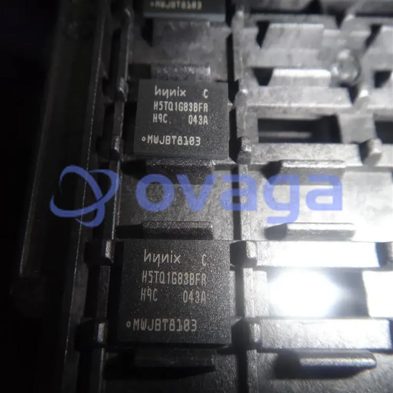
$5000H5TQ1G83BFR-H9C
Enables faster execution of memory-intensive tasks, ensuring smoother performance in various mobile-related operation


브랜드: SK HYNIX INC
제조업체부품 #: H5TQ1G83BFR-H9C
데이터 시트: H5TQ1G83BFR-H9C 데이터 시트 (PDF)
패키지/케이스: FBGA-78
상품 유형: DRAMs
특징
- VDD=VDDQ=1.5V +/- 0.075V
- Fully differential clock inputs (CK, CK) operation
- Differential Data Strobe (DQS, DQS)
- On chip DLL align DQ, DQS and DQS transition with CK
- transition
- DM masks write data-in at the both rising and falling
- edges of the data strobe
- All addresses and control inputs except data,
- data strobes and data masks latched on the
- rising edges of the clock
- Programmable CAS latency 5, 6, 7, 8, 9, 10, 11, 12, 13
- and 14 supported
- Programmable additive latency 0, CL-1, and CL-2
- supported
- Programmable CAS Write latency (CWL) = 5, 6, 7, 8, 9, 10
- Programmable burst length 4/8 with both nibble
- sequential and interleave mode
- BL switch on the fly
- 8banks
- Average Refresh Cycle (Tcase of0 oC~ 95oC)
- - 7.8 µs at 0oC ~ 85 oC
- - 3.9 µs at 85oC ~ 95 oC
- JEDEC standard 78ball FBGA(x4/x8)
- Driver strength selected by EMRS
- Dynamic On Die Termination supported
- Asynchronous RESET pin supported
- ZQ calibration supported
- TDQS (Termination Data Strobe) supported (x8 only)
- Write Levelization supported
- 8 bit pre-fetch
- This product in compliance with the RoHS directive.
명세서
| 매개변수 | 값 | 매개변수 | 값 |
|---|---|---|---|
| Rohs Code | Yes | Part Life Cycle Code | Obsolete |
| Ihs Manufacturer | SK HYNIX INC | Part Package Code | BGA |
| Package Description | TFBGA, BGA78,9X13,32 | Pin Count | 78 |
| Reach Compliance Code | ECCN Code | EAR99 | |
| HTS Code | 8542.32.00.36 | Access Mode | MULTI BANK PAGE BURST |
| Access Time-Max | 20 ns | Additional Feature | AUTO/SELF REFRESH |
| Clock Frequency-Max (fCLK) | 667 MHz | I/O Type | COMMON |
| Interleaved Burst Length | 4,8 | JESD-30 Code | R-PBGA-B78 |
| JESD-609 Code | e1 | Length | 11 mm |
| Memory Density | 2415919104 bit | Memory IC Type | DDR3 DRAM |
| Memory Width | 18 | Number of Functions | 1 |
| Number of Ports | 1 | Number of Terminals | 78 |
| Number of Words | 134217728 words | Number of Words Code | 128000000 |
| Operating Mode | SYNCHRONOUS | Operating Temperature-Max | 85 °C |
| Operating Temperature-Min | Organization | 128MX18 | |
| Output Characteristics | 3-STATE | Package Body Material | PLASTIC/EPOXY |
| Package Code | TFBGA | Package Equivalence Code | BGA78,9X13,32 |
| Package Shape | RECTANGULAR | Package Style | GRID ARRAY, THIN PROFILE, FINE PITCH |
| Peak Reflow Temperature (Cel) | 260 | Qualification Status | Not Qualified |
| Refresh Cycles | 8192 | Seated Height-Max | 1.2 mm |
| Self Refresh | YES | Sequential Burst Length | 4,8 |
| Supply Current-Max | 0.2 mA | Supply Voltage-Max (Vsup) | 1.575 V |
| Supply Voltage-Min (Vsup) | 1.425 V | Supply Voltage-Nom (Vsup) | 1.5 V |
| Surface Mount | YES | Technology | CMOS |
| Temperature Grade | OTHER | Terminal Finish | Tin/Silver/Copper (Sn96.5Ag3.0Cu0.5) |
| Terminal Form | BALL | Terminal Pitch | 0.8 mm |
| Terminal Position | BOTTOM | Time@Peak Reflow Temperature-Max (s) | 20 |
| Width | 7.5 mm |
배송
| 배송 유형 | 배송비 | 리드타임 | |
|---|---|---|---|
 |
DHL | $20.00-$40.00 (0.50 KG) | 2-5 날 |
 |
페덱스 | $20.00-$40.00 (0.50 KG) | 2-5 날 |
 |
UPS | $20.00-$40.00 (0.50 KG) | 2-5 날 |
 |
TNT | $20.00-$40.00 (0.50 KG) | 2-5 날 |
 |
EMS | $20.00-$40.00 (0.50 KG) | 2-5 날 |
 |
등기 항공 우편 | $20.00-$40.00 (0.50 KG) | 2-5 날 |
처리 시간: 배송비는 지역 및 국가에 따라 다릅니다.
지불
| 지불 조건 | 핸드 수수료 | |
|---|---|---|
 |
은행 송금 | US$30.00의 은행 수수료를 부과합니다. |
 |
페이팔 | 4.0%의 서비스 수수료를 부과합니다. |
 |
신용 카드 | 3.5% 서비스 수수료를 부과합니다. |
 |
웨스턴 유니언 | charge US.00 banking fee. |
 |
돈 그램 | US$0.00의 은행 수수료를 부과합니다. |
보증
1. 귀하가 구입한 전자 부품에는 365일 보증이 포함되어 있으며, 우리는 제품 품질을 보장합니다.
2. 귀하가 받은 품목 중 일부가 완벽한 품질이 아닌 경우, 당사는 책임 있게 귀하의 환불 또는 교체를 준비할 것입니다. 그러나 품목은 원래 상태를 유지해야 합니다.
포장
-

단계1 :제품
-

단계2 :진공 포장
-

단계3 :정전기 방지 가방
-

단계4 :개별 포장
-

단계5 :포장 상자
-

단계6 :바코드 배송 태그


모든 제품은 정전기 방지 가방에 포장됩니다. ESD 정전기 방지 보호 장치와 함께 배송됩니다.
외부 ESD 포장 라벨은 당사 정보(부품 번호, 브랜드 및 수량)를 사용합니다.
우리는 선적 전에 모든 상품을 검사하고, 모든 제품이 양호한 상태인지 확인하고, 부품이 새로운 원본 일치 데이터시트인지 확인합니다.
모든 상품을 포장한 후 문제가 없는지 확인한 후 안전하게 포장하여 글로벌 특급으로 보내드립니다. 우수한 밀봉 무결성과 함께 탁월한 천공 및 인열 저항성을 나타냅니다.


부품 포인트
-
The H5TQ1G83BFR-H9C is a chip commonly used in smartphones and other electronic devices. It is a high-performance, low-power DDR3L SDRAM chip manufactured by SK Hynix. With a capacity of 1 gigabit and a frequency of 933 MHz, it provides fast and efficient memory access for improved device performance.
-
Features
H5TQ1G83BFR-H9C is a DDR4 SDRAM chip manufactured by SK Hynix. It has a capacity of 1 gigabit, operates at a speed of 2400 MHz, and is designed to be used in high-performance computing systems. It features low power consumption and high data transfer rates, making it suitable for various applications. -
Pinout
The H5TQ1G83BFR-H9C is a DDR3 SDRAM chip with a pin count of 60. Its main function is to provide storage capacity and fast data transfer rates for computing devices, such as smartphones, tablets, and other electronic devices. -
Manufacturer
H5TQ1G83BFR-H9C is manufactured by SK Hynix, a South Korean semiconductor company. It is one of the world's largest manufacturers of memory chips, including DRAM and NAND flash, and a leading provider of various semiconductor solutions for mobile devices, computers, servers, and more. -
Application Field
The H5TQ1G83BFR-H9C is a high-performance DDR2 SDRAM memory component. It can be used in various electronic devices such as smartphones, tablets, portable gaming consoles, and networking equipment to enhance their memory and processing capabilities. -
Package
The H5TQ1G83BFR-H9C chip has a package type of BGA (Ball Grid Array), a form factor of FBGA (Fine Ball Grid Array), and a size of 11.5mm x 13mm.


우리는 고품질 제품, 사려 깊은 서비스 및 판매 후 보증을 제공합니다.
-

우리는 풍부한 제품을 보유하고 있으며 귀하의 다양한 요구를 충족시킬 수 있습니다.
-

최소 주문 수량은 1개부터입니다.
-

최저 국제 배송비는 $0.00부터 시작됩니다
-

모든 제품에 대해 365일 품질 보증


