이미지는 참고용입니다. 제품 사양 보기
주문 금액이
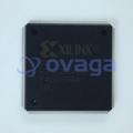
$5000Xilinx XC7K325T-1FFG900C
The XC7K325T-1FFG900C FPGA is part of the KINTEX-7 family, featuring 350 logic cells and a FCBGA-900 package


브랜드: AMD Xilinx, Inc
제조업체부품 #: XC7K325T-1FFG900C
데이터 시트: XC7K325T-1FFG900C Datasheet (PDF)
패키지/케이스: BGA-900
XC7K325T-1FFG900C 일반적인 설명
When it comes to FPGA design, the XC7K325T-1FFG900C from Xilinx stands out for its impressive specifications and features. With a total of 50950 logic blocks and 326080 macrocells, this FPGA offers ample resources for implementing complex designs. The 350 I/Os provide flexibility for connecting external devices, while the FCBGA package and 900 pins make it easy to integrate into your system. The XC7K325T-1FFG900C is also RoHS compliant, demonstrating Xilinx's commitment to environmental sustainability
특징
- "XC" stands for Xilinx FPGA
- "7" stands for the 7-series FPGA family
- "K" stands for the Kintex-7 sub-family
- "325" refers to the number of logic cells (i.e. basic building blocks) in the FPGA
- "T" indicates that it is designed for a specific temperature range (i.e. commercial grade)
- "-1" indicates the speed grade of the device
- "FFG900C" refers to the package type, pin count, and speed grade.
애플리케이션
- 325,200 logic cells
- 21,560 Kb block RAM
- 1,620 DSP slices
- 520 I/O pins
- Maximum clock frequency of 400 MHz
- Configurable logic block (CLB) architecture
명세서
| 매개변수 | 값 | 매개변수 | 값 |
|---|---|---|---|
| Case/Package | FCBGA | Contact Plating | Copper, Silver, Tin |
| Number of Pins | 900 | Max Operating Temperature | 85 °C |
| Max Supply Voltage | 1.03 V | Memory Size | 1 GB |
| Memory Type | DDR3 | Min Operating Temperature | 0 °C |
| Min Supply Voltage | 970 mV | Number of ADC Channels | 1 |
| Number of I/Os | 500 | Number of Logic Blocks (LABs) | 25475 |
| Number of Logic Elements/Cells | 326080 | Number of Registers | 407600 |
| Number of Transceivers | 16 | RAM Size | 2 MB |
| Speed Grade | -1 | Length | 31 mm |
| Width | 31 mm |
배송
| 배송 유형 | 배송비 | 리드타임 | |
|---|---|---|---|
 |
DHL | $20.00-$40.00 (0.50 KG) | 2-5 날 |
 |
페덱스 | $20.00-$40.00 (0.50 KG) | 2-5 날 |
 |
UPS | $20.00-$40.00 (0.50 KG) | 2-5 날 |
 |
TNT | $20.00-$40.00 (0.50 KG) | 2-5 날 |
 |
EMS | $20.00-$40.00 (0.50 KG) | 2-5 날 |
 |
등기 항공 우편 | $20.00-$40.00 (0.50 KG) | 2-5 날 |
처리 시간: 배송비는 지역 및 국가에 따라 다릅니다.
지불
| 지불 조건 | 핸드 수수료 | |
|---|---|---|
 |
은행 송금 | US$30.00의 은행 수수료를 부과합니다. |
 |
페이팔 | 4.0%의 서비스 수수료를 부과합니다. |
 |
신용 카드 | 3.5% 서비스 수수료를 부과합니다. |
 |
웨스턴 유니언 | charge US.00 banking fee. |
 |
돈 그램 | US$0.00의 은행 수수료를 부과합니다. |
보증
1. 귀하가 구입한 전자 부품에는 365일 보증이 포함되어 있으며, 우리는 제품 품질을 보장합니다.
2. 귀하가 받은 품목 중 일부가 완벽한 품질이 아닌 경우, 당사는 책임 있게 귀하의 환불 또는 교체를 준비할 것입니다. 그러나 품목은 원래 상태를 유지해야 합니다.
포장
-

단계1 :제품
-

단계2 :진공 포장
-

단계3 :정전기 방지 가방
-

단계4 :개별 포장
-

단계5 :포장 상자
-

단계6 :바코드 배송 태그


모든 제품은 정전기 방지 가방에 포장됩니다. ESD 정전기 방지 보호 장치와 함께 배송됩니다.
외부 ESD 포장 라벨은 당사 정보(부품 번호, 브랜드 및 수량)를 사용합니다.
우리는 선적 전에 모든 상품을 검사하고, 모든 제품이 양호한 상태인지 확인하고, 부품이 새로운 원본 일치 데이터시트인지 확인합니다.
모든 상품을 포장한 후 문제가 없는지 확인한 후 안전하게 포장하여 글로벌 특급으로 보내드립니다. 우수한 밀봉 무결성과 함께 탁월한 천공 및 인열 저항성을 나타냅니다.


등가 부품
에 대한 XC7K325T-1FFG900C 구성 요소인 경우 이러한 교체 및 대체 부품을 고려할 수 있습니다.:
부품 번호
브랜드
패키지
설명
부품 번호 : Image
브랜드 :
패키지 :
설명 : processing
부품 번호 : High-speed
브랜드 :
패키지 :
설명 : data communication
부품 번호 : Encryption
브랜드 :
패키지 :
설명 : and security
부품 번호 : System
브랜드 :
패키지 :
설명 : monitoring and control
부품 번호 : Protocol
브랜드 :
패키지 :
설명 : bridging and conversion
부품 포인트
-
XC7K325T-1FFG900C is a field-programmable gate array (FPGA) chip manufactured by Xilinx. It belongs to the Kintex-7 family and offers a high-density and high-performance solution for various applications. Its unique features include a large number of programmable logic cells, high-speed transceivers, and DSP slices. The chip is widely used in sectors like aerospace, defense, communication, and industrial automation for its versatility and reliability.
-
Equivalent
There are no direct equivalents to the XC7K325T-1FFG900C chip. However, similar alternatives include Xilinx Kintex-7 FPGAs such as XC7K325T-2FFG900C, XC7K325T-2FFG900I, and XC7K325T-3FFG900C, which offer similar performance and features. -
Features
XC7K325T-1FFG900C is a high-performance field-programmable gate array (FPGA) with 324,000 logic cells, 4,080 Kb block RAM, and 2,240 DSP slices. It operates at a speed grade of -1 and has a 900-pin flip-chip package. The FPGA is built on a 28nm technology, offering high performance, low power consumption, and extensive programmability for various applications. -
Pinout
The XC7K325T-1FFG900C is a field programmable gate array (FPGA) from the Xilinx Kintex-7 family. It has a pin count of 900 and its functions can be programmed to perform various logic operations and tasks. -
Manufacturer
The manufacturer of the XC7K325T-1FFG900C is Xilinx Inc. It is an American technology company specializing in the design and production of programmable logic devices such as field-programmable gate arrays (FPGAs). -
Application Field
The XC7K325T-1FFG900C FPGA is commonly used in various application areas such as aerospace and defense, wired communications, video and image processing, and high-performance computing. It is known for its versatility, reliability, and high-speed processing capabilities, making it suitable for a wide range of demanding applications. -
Package
The XC7K325T-1FFG900C is a chip that belongs to the Xilinx 7 series (XC7) family. It has a package type of flip-chip ball grid array (BGA) and a form factor of 900 CBGA. The size of the chip can be inferred from its package type and form factor.


데이터 시트 PDF
우리는 고품질 제품, 사려 깊은 서비스 및 판매 후 보증을 제공합니다.
-

우리는 풍부한 제품을 보유하고 있으며 귀하의 다양한 요구를 충족시킬 수 있습니다.
-

최소 주문 수량은 1개부터입니다.
-

최저 국제 배송비는 $0.00부터 시작됩니다
-

모든 제품에 대해 365일 품질 보증