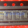
이미지는 참고용입니다. 제품 사양 보기
주문 금액이
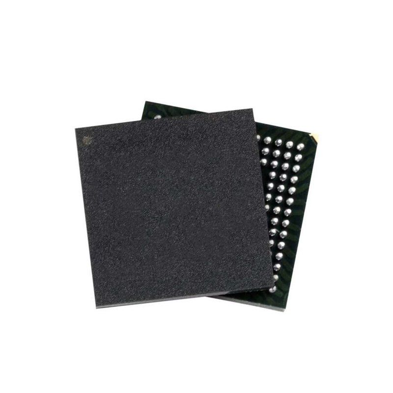
$5000WINBOND W631GG6KB15K
DRAM Chip DDR3 SDRAM 1Gbit 64Mx16 1.5V96-Pin WBGA


W631GG6KB15K 일반적인 설명
GENERAL DESCRIPTIONThe W631GG6KB is a 1G bits DDR3 SDRAM, organized as 8,388,608 words x 8 banks x 16 bits. This device achieves high speed transfer rates up to 1866 Mb/sec/pin (DDR3-1866) for various applications. W631GG6KB is sorted into the following speed grades: -11, -12, 12I, 12A, 12K -15, 15I, 15A and 15K. The -11 speed grade is compliant to the DDR3-1866 (13-13-13) specification. The -12, 12I, 12A and 12K speed grades are compliant to the DDR3-1600 (11-11-11) specification (the 12I industrial grade which is guaranteed to support -40°C ≤ TCASE ≤ 95°C). The -15, 15I, 15A and 15K speed grades are compliant to the DDR3-1333 (9-9-9) specification (the 15I industrial grade which is guaranteed to support -40°C ≤ TCASE ≤ 95°C).FEATURES Power Supply: VDD, VDDQ = 1.5V ± 0.075V Double Data Rate architecture: two data transfers per clock cycle Eight internal banks for concurrent operation 8 bit prefetch architecture CAS Latency: 6, 7, 8, 9, 10, 11 and 13 Burst length 8 (BL8) and burst chop 4 (BC4) modes: fixed via mode register (MRS) or selectable On The-Fly (OTF) Programmable read burst ordering: interleaved or nibble sequential Bi-directional, differential data strobes (DQS and DQS#) are transmitted / received with data Edge-aligned with read data and center-aligned with write data DLL aligns DQ and DQS transitions with clock Differential clock inputs (CK and CK#) Commands entered on each positive CK edge, data and data mask are referenced to both edges of a differential data strobe pair (double data rate) Posted CAS with programmable additive latency (AL = 0, CL - 1 and CL - 2) for improved command, address and data bus efficiency Read Latency = Additive Latency plus CAS Latency (RL = AL + CL) Auto-precharge operation for read and write bursts Refresh, Self-Refresh, Auto Self-refresh (ASR) and Partial array self refresh (PASR) Precharged Power Down and Active Power Down
특징
- Power Supply: VDD, VDDQ = 1.5V ± 0.075V
- Double Data Rate architecture: two data transfers per clock cycle
- Eight internal banks for concurrent operation
- 8 bit prefetch architecture
- CAS Latency: 6, 7, 8, 9, 10, 11 and 13
- Burst length 8 (BL8) and burst chop 4 (BC4) modes: fixed via mode register (MRS) or selectable On The-Fly (OTF)
- Programmable read burst ordering: interleaved or nibble sequential
- Bi-directional, differential data strobes (DQS and DQS#) are transmitted / received with data
- Edge-aligned with read data and center-aligned with write data
- DLL aligns DQ and DQS transitions with clock
- Differential clock inputs (CK and CK#)
- Commands entered on each positive CK edge, data and data mask are referenced to both edges of a differential data strobe pair (double data rate)
- Posted CAS with programmable additive latency (AL = 0, CL - 1 and CL - 2) for improved command, address and data bus efficiency
- Read Latency = Additive Latency plus CAS Latency (RL = AL + CL)
- Auto-precharge operation for read and write bursts
- Refresh, Self-Refresh, Auto Self-refresh (ASR) and Partial array self refresh (PASR)
- Precharged Power Down and Active Power Down
명세서
| 매개변수 | 값 | 매개변수 | 값 |
|---|---|---|---|
| EU RoHS | Yes | RoHS Version | 2011/65/EU, 2015/863 |
| ECCN | EAR99 | Automotive | Yes |
| Supplier Cage Code | SDM39 | HTSUSA | 8542320032 |
| Schedule B | 8542320015 |
배송
| 배송 유형 | 배송비 | 리드타임 | |
|---|---|---|---|
 |
DHL | $20.00-$40.00 (0.50 KG) | 2-5 날 |
 |
페덱스 | $20.00-$40.00 (0.50 KG) | 2-5 날 |
 |
UPS | $20.00-$40.00 (0.50 KG) | 2-5 날 |
 |
TNT | $20.00-$40.00 (0.50 KG) | 2-5 날 |
 |
EMS | $20.00-$40.00 (0.50 KG) | 2-5 날 |
 |
등기 항공 우편 | $20.00-$40.00 (0.50 KG) | 2-5 날 |
처리 시간: 배송비는 지역 및 국가에 따라 다릅니다.
지불
| 지불 조건 | 핸드 수수료 | |
|---|---|---|
 |
은행 송금 | US$30.00의 은행 수수료를 부과합니다. |
 |
페이팔 | 4.0%의 서비스 수수료를 부과합니다. |
 |
신용 카드 | 3.5% 서비스 수수료를 부과합니다. |
 |
웨스턴 유니언 | charge US.00 banking fee. |
 |
돈 그램 | US$0.00의 은행 수수료를 부과합니다. |
보증
1. 귀하가 구입한 전자 부품에는 365일 보증이 포함되어 있으며, 우리는 제품 품질을 보장합니다.
2. 귀하가 받은 품목 중 일부가 완벽한 품질이 아닌 경우, 당사는 책임 있게 귀하의 환불 또는 교체를 준비할 것입니다. 그러나 품목은 원래 상태를 유지해야 합니다.
포장
-

단계1 :제품
-

단계2 :진공 포장
-

단계3 :정전기 방지 가방
-

단계4 :개별 포장
-

단계5 :포장 상자
-

단계6 :바코드 배송 태그


모든 제품은 정전기 방지 가방에 포장됩니다. ESD 정전기 방지 보호 장치와 함께 배송됩니다.
외부 ESD 포장 라벨은 당사 정보(부품 번호, 브랜드 및 수량)를 사용합니다.
우리는 선적 전에 모든 상품을 검사하고, 모든 제품이 양호한 상태인지 확인하고, 부품이 새로운 원본 일치 데이터시트인지 확인합니다.
모든 상품을 포장한 후 문제가 없는지 확인한 후 안전하게 포장하여 글로벌 특급으로 보내드립니다. 우수한 밀봉 무결성과 함께 탁월한 천공 및 인열 저항성을 나타냅니다.


우리는 고품질 제품, 사려 깊은 서비스 및 판매 후 보증을 제공합니다.
-

우리는 풍부한 제품을 보유하고 있으며 귀하의 다양한 요구를 충족시킬 수 있습니다.
-

최소 주문 수량은 1개부터입니다.
-

최저 국제 배송비는 $0.00부터 시작됩니다
-

모든 제품에 대해 365일 품질 보증