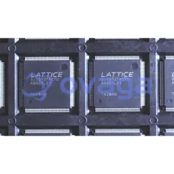
이미지는 참고용입니다. 제품 사양 보기
주문 금액이
$5000LATTICE LFXP2-8E-5FTN256I
FPGA featuring 8,000 LUTs, 201 I/O interfaces, and an integrated DSP unit, designed for operation at a speed grade of -5 with a voltage of 1.2V


LFXP2-8E-5FTN256I 일반적인 설명
The Lattice Semiconductor LFXP2-8E-5FTN256I FPGA is a powerhouse of technology, boasting 2,016 LUTs, 9,216 flip-flops, and 18 multipliers. This FPGA is a top choice for high-performance applications that demand efficiency and speed. Its compact 256-pin FBGA package makes it ideal for space-constrained designs, while its 1.2V core voltage ensures low power consumption. With embedded block RAM, PLLs, and SERDES capabilities, this FPGA is well-equipped for a range of tasks, from clock management to high-speed data communication. Its support for multiple I/O standards adds versatility to its already impressive array of features
특징
- Fully supports PowerPC™ 60x bus protocol, include PowerPC 603, 604, 740, 750 and 8260.
- Supports up to eight PowerPC bus masters with unlimited slave device support.
- Supports two outstanding bus accesses.
- Supports address only transfer and address bus retry.
- Independent address bus and data bus tenure with separate bus grant and data bus grant.
- Option for fixed priority assignment or rotating priority scheme.
- Designed for ASIC or programmable logic device implementations in various system environments.
- Fully static design with edge triggered flip-flops.
- Optimized for ispXPGA product family.

명세서
| 매개변수 | 값 | 매개변수 | 값 |
|---|---|---|---|
| Manufacturer: | Lattice | Product Category: | FPGA - Field Programmable Gate Array |
| RoHS: | Details | Series: | LFXP2 |
| Number of Logic Elements: | 8000 LE | Adaptive Logic Modules - ALMs: | 4000 ALM |
| Embedded Memory: | 221 kbit | Number of I/Os: | 201 I/O |
| Supply Voltage - Min: | 1.14 V | Supply Voltage - Max: | 1.26 V |
| Minimum Operating Temperature: | - 40 C | Maximum Operating Temperature: | + 100 C |
| Mounting Style: | SMD/SMT | Package / Case: | FTBGA-256 |
| Packaging: | Tray | Brand: | Lattice |
| Distributed RAM: | 18 kbit | Embedded Block RAM - EBR: | 221 kbit |
| Height: | 1.25 mm | Length: | 17 mm |
| Maximum Operating Frequency: | 311 MHz | Moisture Sensitive: | Yes |
| Number of Logic Array Blocks - LABs: | 1000 LAB | Operating Supply Voltage: | 1.2 V |
| Product Type: | FPGA - Field Programmable Gate Array | Factory Pack Quantity: | 90 |
| Subcategory: | Programmable Logic ICs | Total Memory: | 239 kbit |
| Width: | 17 mm |
배송
| 배송 유형 | 배송비 | 리드타임 | |
|---|---|---|---|
 |
DHL | $20.00-$40.00 (0.50 KG) | 2-5 날 |
 |
페덱스 | $20.00-$40.00 (0.50 KG) | 2-5 날 |
 |
UPS | $20.00-$40.00 (0.50 KG) | 2-5 날 |
 |
TNT | $20.00-$40.00 (0.50 KG) | 2-5 날 |
 |
EMS | $20.00-$40.00 (0.50 KG) | 2-5 날 |
 |
등기 항공 우편 | $20.00-$40.00 (0.50 KG) | 2-5 날 |
처리 시간: 배송비는 지역 및 국가에 따라 다릅니다.
지불
| 지불 조건 | 핸드 수수료 | |
|---|---|---|
 |
은행 송금 | US$30.00의 은행 수수료를 부과합니다. |
 |
페이팔 | 4.0%의 서비스 수수료를 부과합니다. |
 |
신용 카드 | 3.5% 서비스 수수료를 부과합니다. |
 |
웨스턴 유니언 | charge US.00 banking fee. |
 |
돈 그램 | US$0.00의 은행 수수료를 부과합니다. |
보증
1. 귀하가 구입한 전자 부품에는 365일 보증이 포함되어 있으며, 우리는 제품 품질을 보장합니다.
2. 귀하가 받은 품목 중 일부가 완벽한 품질이 아닌 경우, 당사는 책임 있게 귀하의 환불 또는 교체를 준비할 것입니다. 그러나 품목은 원래 상태를 유지해야 합니다.
포장
-

단계1 :제품
-

단계2 :진공 포장
-

단계3 :정전기 방지 가방
-

단계4 :개별 포장
-

단계5 :포장 상자
-

단계6 :바코드 배송 태그


모든 제품은 정전기 방지 가방에 포장됩니다. ESD 정전기 방지 보호 장치와 함께 배송됩니다.
외부 ESD 포장 라벨은 당사 정보(부품 번호, 브랜드 및 수량)를 사용합니다.
우리는 선적 전에 모든 상품을 검사하고, 모든 제품이 양호한 상태인지 확인하고, 부품이 새로운 원본 일치 데이터시트인지 확인합니다.
모든 상품을 포장한 후 문제가 없는지 확인한 후 안전하게 포장하여 글로벌 특급으로 보내드립니다. 우수한 밀봉 무결성과 함께 탁월한 천공 및 인열 저항성을 나타냅니다.


부품 포인트
-
The LFXP2-8E-5FTN256I is a low power, low-cost field-programmable gate array (FPGA) chip from Lattice Semiconductor. It features 2,100 Look-Up Tables (LUTs), 8,000 logic cells, and offers 5 V operation. The chip is ideal for a wide range of applications including industrial control, automotive, and consumer electronics.
-
Equivalent
Some equivalent products of LFXP2-8E-5FTN256I chip are LFXP2-8E-5MN132I, LFXP2-8E-5TN144I, LFXP2-8E-5MN208I, and LFXP2-8E-5FTN256E. These chips are all from the Lattice FPGA series and have similar specifications and features to the LFXP2-8E-5FTN256I chip. -
Features
The LFXP2-8E-5FTN256I is a low-cost, low FPGA featuring 8500 logic elements, 240 Kbits of RAM, and user I/Os. It supports up to eight high-speed transceivers and is for applications such as video processing, motor control, and communication interfaces. The device also non-volatile configuration memory for easy deployment in embedded systems. -
Pinout
The LFXP2-8E-5FTN256I has a pin count of 256 pins. It is a Field-Programmable Gate Array (FPGA) with 8,000 LUTs, 90 Kbits of memory, and integrated clock management. It is designed for applications requiring low power consumption and high performance. -
Manufacturer
The LFXP2-8E-5FTN256I is manufactured by Lattice Semiconductor Corporation. Lattice Semiconductor Corporation is a fabless semiconductor company that produces programmable logic devices and associated software. It is a technology company that specializes in providing customizable FPGA solutions for various applications including telecommunications, automotive, industrial, and consumer electronics. -
Application Field
The LFXP2-8E-5FTN256I is commonly used in embedded control and sensor applications, industrial automation, automotive electronics, and consumer electronics. Its high reliability, low power consumption, and small form factor make it ideal for applications requiring high performance and energy efficiency in a compact package. -
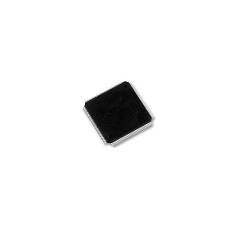
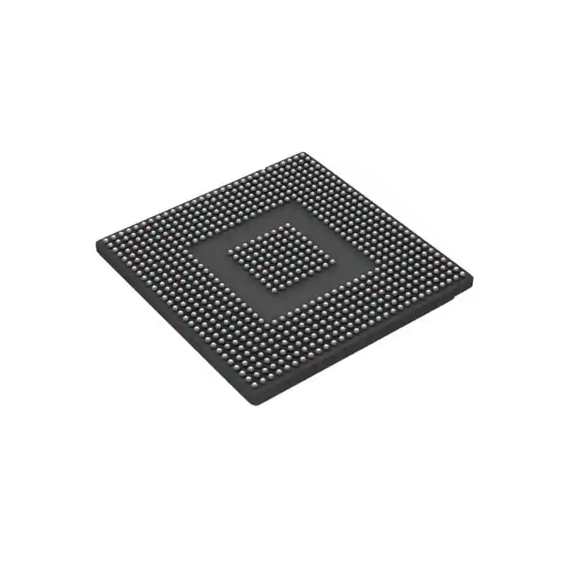
Package
The LFXP2-8E-5FTN256I chip is a Field Programmable Gate Array (FPGA) with a surface mount form factor. It comes in a 256-pin FineLine BGA (Ball Grid Array) package, with dimensions of 17x17mm.


우리는 고품질 제품, 사려 깊은 서비스 및 판매 후 보증을 제공합니다.
-

우리는 풍부한 제품을 보유하고 있으며 귀하의 다양한 요구를 충족시킬 수 있습니다.
-

최소 주문 수량은 1개부터입니다.
-

최저 국제 배송비는 $0.00부터 시작됩니다
-

모든 제품에 대해 365일 품질 보증