이미지는 참고용입니다. 제품 사양 보기
주문 금액이
$5000
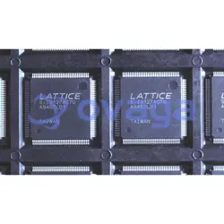
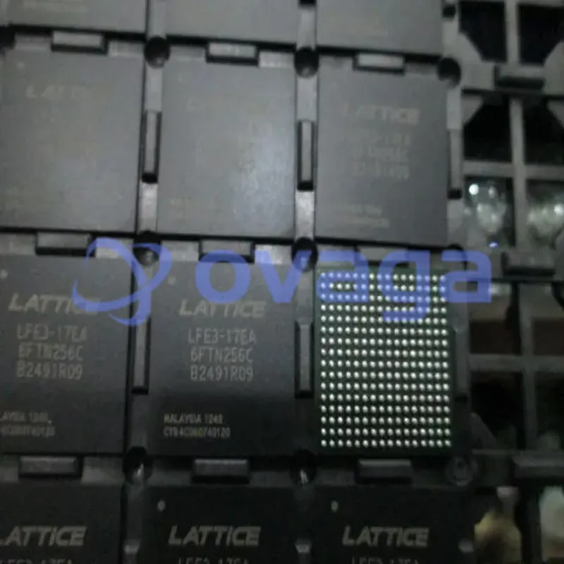
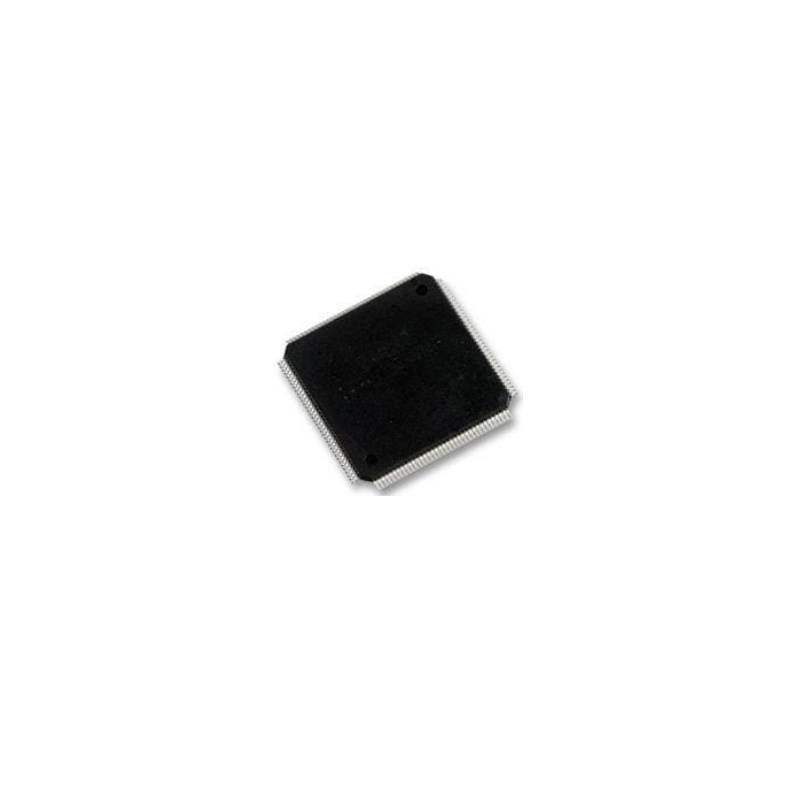
LATTICE LFE3-17EA-6FTN256C

Latticeecp3 ; 17K Luts; 1.2V Rohs Compliant: Yes |Lattice Semiconductor LFE3-17EA-6FTN256C


브랜드: Lattice
제조업체부품 #: LFE3-17EA-6FTN256C
데이터 시트: LFE3-17EA-6FTN256C 데이터 시트 (PDF)
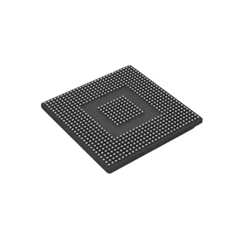
패키지/케이스: FPBGA-256
RoHS 상태:
재고상태: 9,458 PC, 새로운 원본
상품 유형: FPGAs (Field Programmable Gate Array)
Warranty: 1 Year Ovaga Warranty - Find Out More
0
1
*모든 가격은 USD 단위입니다.
| 수량 | 단가 | 추가 가격 |
|---|---|---|
| 1 | $8.664 | $8.664 |
| 10 | $7.634 | $76.340 |
| 30 | $7.008 | $210.240 |
| 100 | $6.481 | $648.100 |
재고: 9,458 PCS
LFE3-17EA-6FTN256C 일반적인 설명
Operating at a maximum clock frequency of 550 MHz and with a 1.2V core voltage, the LFE3-17EA-6FTN256C delivers high performance in a compact 256-pin FineLine BGA package. This makes it ideal for applications where space is limited, without compromising on functionality. Additionally, the FPGA includes advanced security features like bitstream encryption and region lockdown, ensuring that your design IP remains protected
특징
- Higher Logic Density for Increased System Integration
- 17K to 149K LUTs
- 116 to 586 I/Os
- Embedded SERDES
- 150 Mbps to 3.2 Gbps for Generic 8b10b, 10-bit SERDES, and 8-bit SERDES modes
- Data Rates 230 Mbps to 3.2 Gbps per channel for all other protocols
- Up to 16 channels per device: PCI Express, SONET/SDH, Ethernet (1GbE, SGMII, XAUI), CPRI, SMPTE 3G and Serial RapidIO
- sysDSP™
- Fully cascadable slice architecture
- 12 to 160 slices for high performance multiply and accumulate
- Powerful 54-bit ALU operations
- Time Division Multiplexing MAC Sharing
- Rounding and truncation
- Each slice supports
- — Half 36x36, two 18x18 or four 9x9 multipliers
- — Advanced 18x36 MAC and 18x18 Multiply-Multiply-Accumulate (MMAC) operations
- Flexible Memory Resources
- Up to 6.85Mbits sysMEM™ Embedded Block RAM (EBR)
- 36K to 303K bits distributed RAM
- sysCLOCK Analog PLLs and DLLs
- Two DLLs and up to ten PLLs per device
- Pre-Engineered Source Synchronous I/O
- DDR registers in I/O cells
- Dedicated read/write levelling functionality
- Dedicated gearing logic
- Source synchronous standards support
- — ADC/DAC, 7:1 LVDS, XGMII
- — High Speed ADC/DAC devices
- Dedicated DDR/DDR2/DDR3 memory with DQS support
- Optional Inter-Symbol Interference (ISI) correction on outputs
- Programmable sysI/O™ Buffer Supports Wide Range of Interfaces
- On-chip termination
- Optional equalization filter on inputs
- LVTTL and LVCMOS 33/25/18/15/12
- SSTL 33/25/18/15 I, II
- HSTL15 I and HSTL18 I, II
- PCI and Differential HSTL, SSTL
- LVDS, Bus-LVDS, LVPECL, RSDS, MLVDS
- Flexible Device Configuration
- Dedicated bank for configuration I/Os
- SPI boot flash interface
- Dual-boot images supported
- Slave SPI
- TransFR™ I/O for simple field updates
- Soft Error Detect embedded macro
- System Level Support
- IEEE 1149.1 and IEEE 1532 compliant
- Reveal Logic Analyzer
- ORCAstra FPGA configuration utility
- On-chip oscillator for initialization & general use
- 1.2 V core power supply

명세서
| 매개변수 | 값 | 매개변수 | 값 |
|---|---|---|---|
| Manufacturer: | Lattice | Product Category: | FPGA - Field Programmable Gate Array |
| RoHS: | Details | Series: | LFE3 |
| Number of Logic Elements: | 17000 LE | Adaptive Logic Modules - ALMs: | 8500 ALM |
| Embedded Memory: | 700 kbit | Number of I/Os: | 133 I/O |
| Supply Voltage - Min: | 1.14 V | Supply Voltage - Max: | 1.26 V |
| Minimum Operating Temperature: | 0 C | Maximum Operating Temperature: | + 85 C |
| Data Rate: | 3.2 Gb/s | Mounting Style: | SMD/SMT |
| Package / Case: | FPBGA-256 | Packaging: | Tray |
| Brand: | Lattice | Distributed RAM: | 36 kbit |
| Embedded Block RAM - EBR: | 700 kbit | Maximum Operating Frequency: | 375 MHz |
| Moisture Sensitive: | Yes | Number of Logic Array Blocks - LABs: | 2125 LAB |
| Operating Supply Current: | 18 mA | Operating Supply Voltage: | 1.2 V |
| Product Type: | FPGA - Field Programmable Gate Array | Factory Pack Quantity: | 90 |
| Subcategory: | Programmable Logic ICs | Total Memory: | 736 kbit |
| Unit Weight: | 0.834123 oz |
배송
| 배송 유형 | 배송비 | 리드타임 | |
|---|---|---|---|
 |
DHL | $20.00-$40.00 (0.50 KG) | 2-5 날 |
 |
페덱스 | $20.00-$40.00 (0.50 KG) | 2-5 날 |
 |
UPS | $20.00-$40.00 (0.50 KG) | 2-5 날 |
 |
TNT | $20.00-$40.00 (0.50 KG) | 2-5 날 |
 |
EMS | $20.00-$40.00 (0.50 KG) | 2-5 날 |
 |
등기 항공 우편 | $20.00-$40.00 (0.50 KG) | 2-5 날 |
처리 시간: 배송비는 지역 및 국가에 따라 다릅니다.
지불
| 지불 조건 | 핸드 수수료 | |
|---|---|---|
 |
은행 송금 | US$30.00의 은행 수수료를 부과합니다. |
 |
페이팔 | 4.0%의 서비스 수수료를 부과합니다. |
 |
신용 카드 | 3.5% 서비스 수수료를 부과합니다. |
 |
웨스턴 유니언 | charge US.00 banking fee. |
 |
돈 그램 | US$0.00의 은행 수수료를 부과합니다. |
보증
1. 귀하가 구입한 전자 부품에는 365일 보증이 포함되어 있으며, 우리는 제품 품질을 보장합니다.
2. 귀하가 받은 품목 중 일부가 완벽한 품질이 아닌 경우, 당사는 책임 있게 귀하의 환불 또는 교체를 준비할 것입니다. 그러나 품목은 원래 상태를 유지해야 합니다.
포장
-

단계1 :제품
-

단계2 :진공 포장
-

단계3 :정전기 방지 가방
-

단계4 :개별 포장
-

단계5 :포장 상자
-

단계6 :바코드 배송 태그


모든 제품은 정전기 방지 가방에 포장됩니다. ESD 정전기 방지 보호 장치와 함께 배송됩니다.
외부 ESD 포장 라벨은 당사 정보(부품 번호, 브랜드 및 수량)를 사용합니다.
우리는 선적 전에 모든 상품을 검사하고, 모든 제품이 양호한 상태인지 확인하고, 부품이 새로운 원본 일치 데이터시트인지 확인합니다.
모든 상품을 포장한 후 문제가 없는지 확인한 후 안전하게 포장하여 글로벌 특급으로 보내드립니다. 우수한 밀봉 무결성과 함께 탁월한 천공 및 인열 저항성을 나타냅니다.


부품 포인트
-
The LFE3-17EA-6FTN256C chip is a field-programmable gate array (FPGA) produced by Lattice Semiconductor. It features a 17K LUT (Look-Up Table) architecture and uses a 40 nm process technology. This high-performance chip offers low power consumption, excellent system integration, and is suitable for a wide range of applications in industries such as communications, automotive, and industrial automation.
-
Equivalent
The equivalent products of LFE3-17EA-6FTN256C chip include LFE3-17EA-6FN484C, LFE3-17EA-6FTG256C, and LFE3-17EA-6LN256C. -
Features
The LFE3-17EA-6FTN256C is a low-power, field-programmable gate array (FPGA) by Lattice Semiconductor. It offers 17,076 Look-Up Tables (LUTs), 58.8Kb Distributed Memory, 3.5Kb RAM, 64-bit DDR3 memory interface, and 256-ball fine pitch BGA package. It supports up to 293 input/outputs (IOs) with various additional features for efficient design implementation. -
Pinout
The LFE3-17EA-6FTN256C is an FPGA (Field-Programmable Gate Array) with a pin count of 256. It is part of the Lattice ECP3 family and offers a range of general-purpose I/O (Input/Output) functions. -
Manufacturer
The manufacturer of the LFE3-17EA-6FTN256C is Lattice Semiconductor Corporation. It is a semiconductor company that specializes in programmable logic devices, such as field-programmable gate arrays (FPGAs), and related software development tools. -
Application Field
The application areas of the LFE3-17EA-6FTN256C include communication systems, video and image processing, industrial automation, automotive systems, and medical equipment. It is a low-power FPGA with high processing capability, making it suitable for a wide range of applications that require high-performance and low-power consumption. -
Package
The LFE3-17EA-6FTN256C chip comes in a FBGA (Fine-pitch Ball Grid Array) package type. Its form factor is 17 x 17 mm, and it has a size of 289 square millimeters.


우리는 고품질 제품, 사려 깊은 서비스 및 판매 후 보증을 제공합니다.
-

우리는 풍부한 제품을 보유하고 있으며 귀하의 다양한 요구를 충족시킬 수 있습니다.
-

최소 주문 수량은 1개부터입니다.
-

최저 국제 배송비는 $0.00부터 시작됩니다
-

모든 제품에 대해 365일 품질 보증