이미지는 참고용입니다. 제품 사양 보기
주문 금액이
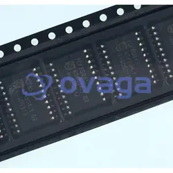
$5000DS90C124
5-MHz to 35-MHz DC-balanced 24-bit FPD-Link II deserializer


브랜드: NS
제조업체부품 #: DS90C124
데이터 시트: DS90C124 데이터 시트 (PDF)
패키지/케이스: TQFP-48
상품 유형: Serializers, Deserializers
DS90C124 일반적인 설명
The DS90C241 and DS90C124 chipset translates a 24-bit parallel bus into a fully transparent data and control LVDS serial stream with embedded clock information. This single serial stream simplifies transferring a 24-bit bus over PCB traces or over cable by eliminating the skew problems between parallel data and clock paths. It saves system cost by narrowing data paths, which in turn reduces PCB layers, cable width, and connector size and pins.
The DS90C241 and DS90C124 incorporate LVDS signaling on the high-speed I/O. LVDS provides a low-power and low-noise environment for reliably transferring data over a serial transmission path. By optimizing the serializer output edge rate for the operating frequency range, EMI is further reduced.
In addition, the device features pre-emphasis to boost signals over longer distances using lossy cables. Internal DC balanced encoding and decoding supports AC-coupled interconnects.
특징
- 5-MHz to 35-MHz Clock Embedded and DC-Balancing 24:1 and 1:24 Data Transmissions
- User Defined Pre-Emphasis Driving Ability Through External Resistor on LVDS Outputs and Capable to Drive Up to 10-Meter Shielded Twisted-Pair Cable
- User-Selectable Clock Edge for Parallel Data on Both Transmitter and Receiver
- Internal DC Balancing Encode and Decode (Supports AC-Coupling Interface With No External Coding Required)
- Individual Power-Down Controls for Both Transmitter and Receiver
- Embedded Clock CDR (Clock and Data Recovery) on Receiver and No External Source of Reference Clock Required
- All Codes RDL (Random Data Lock) to Support Live-Pluggable Applications
- LOCK Output Flag to Ensure Data Integrity at Receiver Side
- Balanced TSETUP and THOLD Between RCLK and RDATA on Receiver Side
- PTO (Progressive Turnon) LVCMOS Outputs to Reduce EMI and Minimize SSO Effects
- All LVCMOS Inputs and Control Pins Have Internal Pulldown
- On-Chip Filters for PLLs on Transmitter and Receiver
- Temperature Range: –40°C to 105°C
- Greater Than 8-kV HBM ESD Tolerant
- Meets AEC-Q100 Compliance
- Power Supply Range: 3.3 V ± 10%
- 48-Pin TQFP Package
배송
| 배송 유형 | 배송비 | 리드타임 | |
|---|---|---|---|
 |
DHL | $20.00-$40.00 (0.50 KG) | 2-5 날 |
 |
페덱스 | $20.00-$40.00 (0.50 KG) | 2-5 날 |
 |
UPS | $20.00-$40.00 (0.50 KG) | 2-5 날 |
 |
TNT | $20.00-$40.00 (0.50 KG) | 2-5 날 |
 |
EMS | $20.00-$40.00 (0.50 KG) | 2-5 날 |
 |
등기 항공 우편 | $20.00-$40.00 (0.50 KG) | 2-5 날 |
처리 시간: 배송비는 지역 및 국가에 따라 다릅니다.
지불
| 지불 조건 | 핸드 수수료 | |
|---|---|---|
 |
은행 송금 | US$30.00의 은행 수수료를 부과합니다. |
 |
페이팔 | 4.0%의 서비스 수수료를 부과합니다. |
 |
신용 카드 | 3.5% 서비스 수수료를 부과합니다. |
 |
웨스턴 유니언 | charge US.00 banking fee. |
 |
돈 그램 | US$0.00의 은행 수수료를 부과합니다. |
보증
1. 귀하가 구입한 전자 부품에는 365일 보증이 포함되어 있으며, 우리는 제품 품질을 보장합니다.
2. 귀하가 받은 품목 중 일부가 완벽한 품질이 아닌 경우, 당사는 책임 있게 귀하의 환불 또는 교체를 준비할 것입니다. 그러나 품목은 원래 상태를 유지해야 합니다.
포장
-

단계1 :제품
-

단계2 :진공 포장
-

단계3 :정전기 방지 가방
-

단계4 :개별 포장
-

단계5 :포장 상자
-

단계6 :바코드 배송 태그


모든 제품은 정전기 방지 가방에 포장됩니다. ESD 정전기 방지 보호 장치와 함께 배송됩니다.
외부 ESD 포장 라벨은 당사 정보(부품 번호, 브랜드 및 수량)를 사용합니다.
우리는 선적 전에 모든 상품을 검사하고, 모든 제품이 양호한 상태인지 확인하고, 부품이 새로운 원본 일치 데이터시트인지 확인합니다.
모든 상품을 포장한 후 문제가 없는지 확인한 후 안전하게 포장하여 글로벌 특급으로 보내드립니다. 우수한 밀봉 무결성과 함께 탁월한 천공 및 인열 저항성을 나타냅니다.


우리는 고품질 제품, 사려 깊은 서비스 및 판매 후 보증을 제공합니다.
-

우리는 풍부한 제품을 보유하고 있으며 귀하의 다양한 요구를 충족시킬 수 있습니다.
-

최소 주문 수량은 1개부터입니다.
-

최저 국제 배송비는 $0.00부터 시작됩니다
-

모든 제품에 대해 365일 품질 보증