


이미지는 참고용입니다. 제품 사양 보기
주문 금액이
$5000Renesas 8T73S1802NLGI8
Clock Buffer BUFFER WITH DIVIDER


제조업체부품 #: 8T73S1802NLGI8
데이터 시트: 8T73S1802NLGI8 데이터 시트 (PDF)
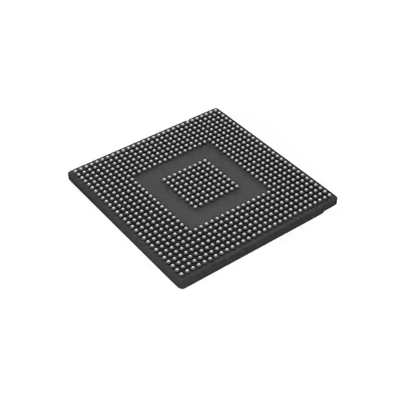
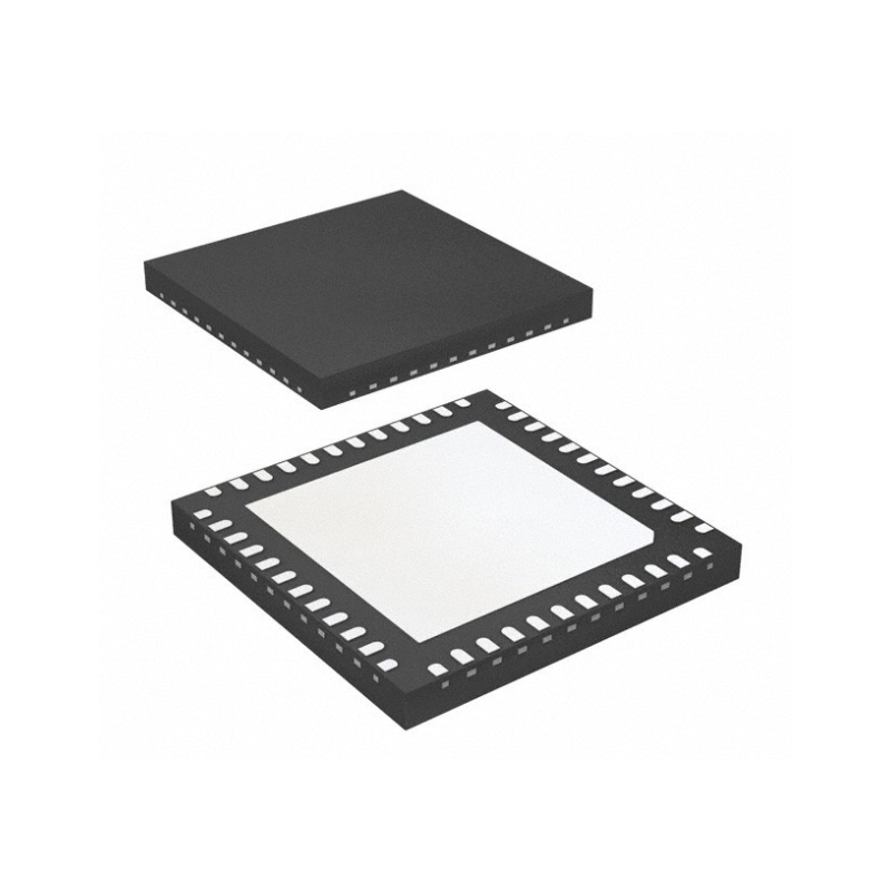
패키지/케이스: Quad Flat No-Lead - NLG16P2-ren1
상품 유형: Clock Buffers, Drivers
8T73S1802NLGI8 일반적인 설명
The 8T73S1802 is a fully integrated clock fanout buffer and frequency divider. The input signal is frequency-divided and then fanned out to one differential LVPECL and one LVCMOS output. Each of the outputs can select its individual divider value from the range of ÷1, ÷2, ÷4 and ÷8. Three control inputs EN, SEL0 and SEL1 (3-level logic) are available to select the frequency dividers and the output enable/disable state. The single-ended LVCMOS output is phase-delayed by 650ps to minimize coupling of LVCMOS switching into the differential output during its signal transition.
The 8T73S1802 is optimized to deliver very low phase noise clocks. The VBB output generates a common-mode voltage reference for the differential clock input so that connecting the VBB pin to an unused input (nCLK) enables to use of single-ended input signals. The extended temperature range supports wireless infrastructure, telecommunication and networking end equipment requirements. The 8T73S1802 can be used with a 3.3V or a 2.5V power supply. The device is a member of the high-performance clock family from IDT.
특징
- High-performance fanout buffer clock and fanout buffer
- Input clock signal is distributed to one LVPECL and one LVCMOS output
- Configurable output dividers for both LVPECL and LVCMOS outputs
- Supports clock frequencies up to 1000MHz (LVPECL) and up to 200MHz (LVCMOS)
- Flexible differential input supports LVPECL, LVDS and CML
- VBB generator output supports single-ended input signal applications
- Optimized for low phase noise
- 650ps delay between LVCMOS and LVPECL minimizes coupling between outputs
- Supply voltage: 3.3V or 2.5V
- -40°C to 85°C ambient operating temperature
- 16 VFQFN package (3mm x 3mm)
명세서
| 매개변수 | 값 | 매개변수 | 값 |
|---|---|---|---|
| Pin Count | 17 | Package Category | Quad Flat No-Lead |
| Released Date | Jan 20, 2020 |
배송
| 배송 유형 | 배송비 | 리드타임 | |
|---|---|---|---|
 |
DHL | $20.00-$40.00 (0.50 KG) | 2-5 날 |
 |
페덱스 | $20.00-$40.00 (0.50 KG) | 2-5 날 |
 |
UPS | $20.00-$40.00 (0.50 KG) | 2-5 날 |
 |
TNT | $20.00-$40.00 (0.50 KG) | 2-5 날 |
 |
EMS | $20.00-$40.00 (0.50 KG) | 2-5 날 |
 |
등기 항공 우편 | $20.00-$40.00 (0.50 KG) | 2-5 날 |
처리 시간: 배송비는 지역 및 국가에 따라 다릅니다.
지불
| 지불 조건 | 핸드 수수료 | |
|---|---|---|
 |
은행 송금 | US$30.00의 은행 수수료를 부과합니다. |
 |
페이팔 | 4.0%의 서비스 수수료를 부과합니다. |
 |
신용 카드 | 3.5% 서비스 수수료를 부과합니다. |
 |
웨스턴 유니언 | charge US.00 banking fee. |
 |
돈 그램 | US$0.00의 은행 수수료를 부과합니다. |
보증
1. 귀하가 구입한 전자 부품에는 365일 보증이 포함되어 있으며, 우리는 제품 품질을 보장합니다.
2. 귀하가 받은 품목 중 일부가 완벽한 품질이 아닌 경우, 당사는 책임 있게 귀하의 환불 또는 교체를 준비할 것입니다. 그러나 품목은 원래 상태를 유지해야 합니다.
포장
-

단계1 :제품
-

단계2 :진공 포장
-

단계3 :정전기 방지 가방
-

단계4 :개별 포장
-

단계5 :포장 상자
-

단계6 :바코드 배송 태그


모든 제품은 정전기 방지 가방에 포장됩니다. ESD 정전기 방지 보호 장치와 함께 배송됩니다.
외부 ESD 포장 라벨은 당사 정보(부품 번호, 브랜드 및 수량)를 사용합니다.
우리는 선적 전에 모든 상품을 검사하고, 모든 제품이 양호한 상태인지 확인하고, 부품이 새로운 원본 일치 데이터시트인지 확인합니다.
모든 상품을 포장한 후 문제가 없는지 확인한 후 안전하게 포장하여 글로벌 특급으로 보내드립니다. 우수한 밀봉 무결성과 함께 탁월한 천공 및 인열 저항성을 나타냅니다.


우리는 고품질 제품, 사려 깊은 서비스 및 판매 후 보증을 제공합니다.
-

우리는 풍부한 제품을 보유하고 있으며 귀하의 다양한 요구를 충족시킬 수 있습니다.
-

최소 주문 수량은 1개부터입니다.
-

최저 국제 배송비는 $0.00부터 시작됩니다
-

모든 제품에 대해 365일 품질 보증


