

이미지는 참고용입니다. 제품 사양 보기
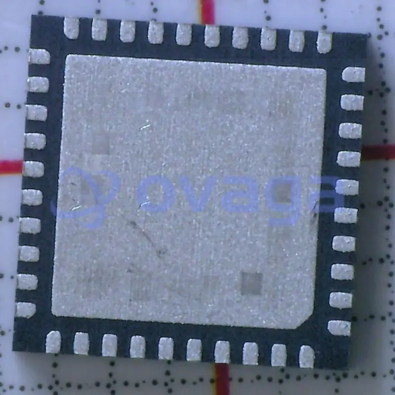
Renesas 8T49N241-998NLGI
Clock Generators & Support Products UFT 1 Integer 3 Frac 0.35ps EEProm 25MHz


제조업체부품 #: 8T49N241-998NLGI
데이터 시트: 8T49N241-998NLGI Datasheet (PDF)
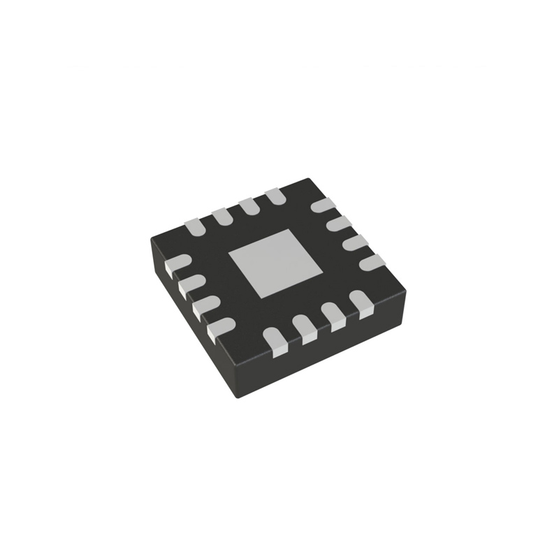
패키지/케이스: VFQFPN-40
상품 유형: Integrated Circuits (ICs)
8T49N241-998NLGI 일반적인 설명
The 8T49N241 has one fractional-feedback PLL that can be used as a frequency translator with jitter attenuation or a frequency synthesizer. It is equipped with one integer and three fractional output dividers, allowing the generation of up to four different and unrelated output frequencies, ranging from 8 kHz to 1 GHz. Output frequencies can be completely independent of the input frequencies, and all four of these frequencies can be completely independent of each other. The four outputs may select among LVPECL, LVDS, HCSL or LVCMOS output levels.
The 8T49N241 is ideal for use in a wide range of equipment, including 10G/40G/100G SONET/SDH and Ethernet network line cards, wireless base station baseband units, broadcast video, carrier Ethernet switches, OTN, or in test and measurement applications. For example, the 8T49N241 can be used in GbE/10GbE/100GbE Synchronous Ethernet line card applications in order to preserve the G.8262 compliance from the Synchronous Equipment Timing Source (SETS) on the timing card.
Renesas’ third generation Universal Frequency Translator family also includes the 8T49N242 (2-in / 1-PLL / 4-out), the 8T49N285 (2-in / 1-PLL / 8-out), the 8T49N286 (4-in / 2-PLL / 8-out) and the 8T49N287 (2-in / 2-PLL / 8-out). These devices are complemented by the 82P33714 and 82P33731 synchronous equipment timing source (SETS) for Synchronous Ethernet (SyncE) and 10G-40G SyncE, respectively.
To see other devices in this product family, visit the Universal Frequency Translators page.
특징
- Compliant with the requirements outlined in Telcordia GR-253-CORE (SONET) & ITU-T G.813/G.8262 (SDH/SONET & SyncE) when paired with a Synchronous Equipment Timing Source (SETS ) device
- Generates up to 4 LVPECL / LVDS/HCSL or 16 LVCMOS output clocks ranging from 8 kHz up to 1.0 GHz (diff), 8 kHz to 250 MHz (LVCMOS), that meet jitter limits for 10G up to 25G Ethernet applications
- 0.35ps RMS (including spurs), 12 kHz to 20 MHz
- Accepts up to two LVPECL, LVDS, LVHSTL, HCSL or LVCMOS input clocks ranging from 8 kHz up to 875 MHz
- Auto and manual input clock selection with hitless switching
- Clock input monitoring, including support for gapped clocks
- Phase-Slope Limiting and Fully Hitless Switching options to control output phase transients
- Operates from a 10 MHz to 50 MHz
- Register programmable through I2C or via external I2C EEPROM
- 8T49N241-998 “Boot from EEPROM”
- 8T49N241-999 “powers up disabled”
- Supported by Renesas Timing Commander Software™
명세서
| 매개변수 | 값 | 매개변수 | 값 |
|---|---|---|---|
| Source Content uid | 8T49N241-998NLGI | Pbfree Code | Yes |
| Rohs Code | Yes | Part Life Cycle Code | Active |
| Ihs Manufacturer | RENESAS ELECTRONICS CORP | Part Package Code | VFQFPN |
| Package Description | VFQFPN-40 | Pin Count | 40 |
| Manufacturer Package Code | NLG40P2 | Reach Compliance Code | compliant |
| ECCN Code | NLR | HTS Code | 8542390001 |
| Samacsys Manufacturer | Renesas Electronics | Additional Feature | IT ALSO OPERATES AT 3.3V NOMINAL SUPPLY |
| JESD-30 Code | S-XQCC-N40 | Moisture Sensitivity Level | 3 |
| Number of Terminals | 40 | Package Body Material | UNSPECIFIED |
| Package Code | HVQCCN | Package Equivalence Code | LCC40,.24SQ,20 |
| Package Shape | SQUARE | Package Style | CHIP CARRIER, HEAT SINK/SLUG, VERY THIN PROFILE |
| Peak Reflow Temperature (Cel) | 260 | Surface Mount | YES |
| Technology | CMOS | Temperature Grade | INDUSTRIAL |
| Terminal Finish | TIN | Terminal Form | NO LEAD |
| Terminal Position | QUAD |
배송
| 배송 유형 | 배송비 | 리드타임 | |
|---|---|---|---|
 |
DHL | $20.00-$40.00 (0.50 KG) | 2-5 날 |
 |
페덱스 | $20.00-$40.00 (0.50 KG) | 2-5 날 |
 |
UPS | $20.00-$40.00 (0.50 KG) | 2-5 날 |
 |
TNT | $20.00-$40.00 (0.50 KG) | 2-5 날 |
 |
EMS | $20.00-$40.00 (0.50 KG) | 2-5 날 |
 |
등기 항공 우편 | $20.00-$40.00 (0.50 KG) | 2-5 날 |
처리 시간: 배송비는 지역 및 국가에 따라 다릅니다.
지불
| 지불 조건 | 핸드 수수료 | |
|---|---|---|
 |
은행 송금 | US$30.00의 은행 수수료를 부과합니다. |
 |
페이팔 | 4.0%의 서비스 수수료를 부과합니다. |
 |
신용 카드 | 3.5% 서비스 수수료를 부과합니다. |
 |
웨스턴 유니언 | charge US.00 banking fee. |
 |
돈 그램 | US$0.00의 은행 수수료를 부과합니다. |
보증
1. 귀하가 구입한 전자 부품에는 365일 보증이 포함되어 있으며, 우리는 제품 품질을 보장합니다.
2. 귀하가 받은 품목 중 일부가 완벽한 품질이 아닌 경우, 당사는 책임 있게 귀하의 환불 또는 교체를 준비할 것입니다. 그러나 품목은 원래 상태를 유지해야 합니다.
포장
-

단계1 :제품
-

단계2 :진공 포장
-

단계3 :정전기 방지 가방
-

단계4 :개별 포장
-

단계5 :포장 상자
-

단계6 :바코드 배송 태그


모든 제품은 정전기 방지 가방에 포장됩니다. ESD 정전기 방지 보호 장치와 함께 배송됩니다.
외부 ESD 포장 라벨은 당사 정보(부품 번호, 브랜드 및 수량)를 사용합니다.
우리는 선적 전에 모든 상품을 검사하고, 모든 제품이 양호한 상태인지 확인하고, 부품이 새로운 원본 일치 데이터시트인지 확인합니다.
모든 상품을 포장한 후 문제가 없는지 확인한 후 안전하게 포장하여 글로벌 특급으로 보내드립니다. 우수한 밀봉 무결성과 함께 탁월한 천공 및 인열 저항성을 나타냅니다.


부품 포인트
-
The 8T49N241-998NLGI chip is a high-performance clock generator designed for applications requiring multiple clock outputs. It offers low jitter and phase noise, supporting various output frequencies. The chip features a flexible I2C interface for configuration and control, along with advanced clocking features and synchronization options. With its compact and efficient design, the 8T49N241-998NLGI chip is suitable for a wide range of applications in the telecommunications, networking, and industrial sectors.
-
Features
The 8T49N241-998NLGI is a clock generator IC that provides 4 differential outputs, with synthesized reference clocks up to 945 MHz. It features programmable output voltage levels, selectable spread spectrum modulation, and multiple clock outputs. Additionally, it supports industrial temperature ranges and low power consumption. -
Pinout
The 8T49N241-998NLGI is a clock generator and jitter attenuator IC. It has 48 pins and is used in applications like networking, telecommunications, and data centers. -
Manufacturer
The manufacturer of the 8T49N241-998NLGI is Integrated Device Technology (IDT). It is a semiconductor company that specializes in designing, developing, and manufacturing various integrated circuits and system-level solutions for a wide range of industries including telecommunications, automotive, consumer electronics, and industrial applications. -
Application Field
The 8T49N241-998NLGI is a timing device used in applications such as telecom equipment, network switches and routers, data storage systems, and industrial automation. It provides precision timing signals necessary for synchronization and clocking in these areas. -
Package
The 8T49N241-998NLGI chip is available in a package type of QFN, a form factor of 3.5 x 3.5 mm, and has a size of 24 pins.
데이터 시트 PDF
우리는 고품질 제품, 사려 깊은 서비스 및 판매 후 보증을 제공합니다.
-

우리는 풍부한 제품을 보유하고 있으며 귀하의 다양한 요구를 충족시킬 수 있습니다.
-

최소 주문 수량은 1개부터입니다.
-

최저 국제 배송비는 $0.00부터 시작됩니다
-

모든 제품에 대해 365일 품질 보증


These resistors are durable, and they arrived pretty quickly.