


이미지는 참고용입니다. 제품 사양 보기
주문 금액이
$5000
Renesas 8N4Q001EG-1015CDI8

Clock Generators & Support Products PROGRAMMABLE 5X7 OSCILLATOR


제조업체부품 #: 8N4Q001EG-1015CDI8
데이터 시트: 8N4Q001EG-1015CDI8 데이터 시트 (PDF)
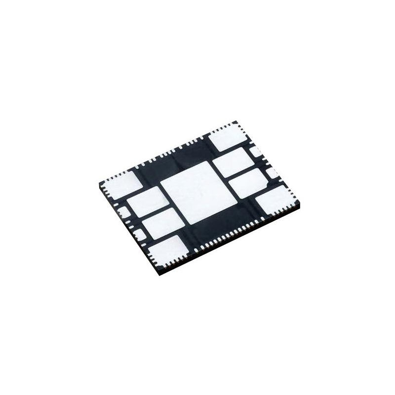
패키지/케이스: Other - CD10
RoHS 상태:
재고상태: 3,235 PC, 새로운 원본
상품 유형: Programmable Timers and Oscillators
Warranty: 1 Year Ovaga Warranty - Find Out More
0
1
*모든 가격은 USD 단위입니다.
| 수량 | 단가 | 추가 가격 |
|---|---|---|
| 1 | $29.896 | $29.896 |
| 200 | $11.570 | $2314.000 |
| 500 | $11.163 | $5581.500 |
| 1000 | $10.962 | $10962.000 |
재고: 3,235 PCS
8N4Q001EG-1015CDI8 일반적인 설명
The 8N4Q001 is a Quad-Frequency Programmable Clock Oscillator with very flexible frequency programming capabilities. The device uses IDT's fourth generation FemtoClock® NG technology for an optimum high clock frequency and low phase noise performance. The device accepts 2.5V or 3.3V supply and is packaged in a small, lead-free (RoHS 6) 10-lead ceramic 5mm x 7mm x 1.55mm package. Besides the four default power-up frequencies set by the FSEL0 and FSEL1 pins, the 8N4Q001 can be programmed via the I2C interface to output clock frequencies between 15.476MHz to 866.67MHz and from 975MHz to 1,300MHz to a very high degree of precision with a frequency step size of 435.9Hz ÷ N (N is the PLL output divider). Since the FSEL0 and FSEL1 pins are mapped to four independent PLL divider registers (P, MINT, MFRAC and N), reprogramming those registers to other frequencies under control of FSEL0 and FSEL1 is supported. The extended temperature range supports wireless infrastructure, telecommunication and networking end equipment requirements.
특징
- Fourth generation FemtoClock® NG technology
- Programmable clock output frequency from 15.476MHz to 866.67MHz and from 975MHz to 1,300MHz
- Four power-up default frequencies (see part number order codes), re-programmable by I2C
- I2C programming interface for the output clock frequency and internal PLL control registers
- Frequency programming resolution is 435.9Hz ÷N
- One 2.5V, 3.3V LVDS clock output
- Two control inputs for the power-up default frequency
- LVCMOS/LVTTL compatible control inputs
- RMS phase jitter @ 156.25MHz (12kHz - 20MHz): 0.253ps (typical), integer PLL feedback configuration
- RMS phase jitter @ 156.25MHz (1kHz - 40MHz): 0.263ps (typical), integer PLL feedback configuration
- Full 2.5V or 3.3V supply modes
- -40°C to 85°C ambient operating temperature
- Available in Lead-free (RoHS 6) package
명세서
| 매개변수 | 값 | 매개변수 | 값 |
|---|---|---|---|
| Pkg. Type | CLCC | Lead Count (#) | 10 |
| Temp. Grade | I | Pb (Lead) Free | Yes |
| Carrier Type | Reel |
배송
| 배송 유형 | 배송비 | 리드타임 | |
|---|---|---|---|
 |
DHL | $20.00-$40.00 (0.50 KG) | 2-5 날 |
 |
페덱스 | $20.00-$40.00 (0.50 KG) | 2-5 날 |
 |
UPS | $20.00-$40.00 (0.50 KG) | 2-5 날 |
 |
TNT | $20.00-$40.00 (0.50 KG) | 2-5 날 |
 |
EMS | $20.00-$40.00 (0.50 KG) | 2-5 날 |
 |
등기 항공 우편 | $20.00-$40.00 (0.50 KG) | 2-5 날 |
처리 시간: 배송비는 지역 및 국가에 따라 다릅니다.
지불
| 지불 조건 | 핸드 수수료 | |
|---|---|---|
 |
은행 송금 | US$30.00의 은행 수수료를 부과합니다. |
 |
페이팔 | 4.0%의 서비스 수수료를 부과합니다. |
 |
신용 카드 | 3.5% 서비스 수수료를 부과합니다. |
 |
웨스턴 유니언 | charge US.00 banking fee. |
 |
돈 그램 | US$0.00의 은행 수수료를 부과합니다. |
보증
1. 귀하가 구입한 전자 부품에는 365일 보증이 포함되어 있으며, 우리는 제품 품질을 보장합니다.
2. 귀하가 받은 품목 중 일부가 완벽한 품질이 아닌 경우, 당사는 책임 있게 귀하의 환불 또는 교체를 준비할 것입니다. 그러나 품목은 원래 상태를 유지해야 합니다.
포장
-

단계1 :제품
-

단계2 :진공 포장
-

단계3 :정전기 방지 가방
-

단계4 :개별 포장
-

단계5 :포장 상자
-

단계6 :바코드 배송 태그


모든 제품은 정전기 방지 가방에 포장됩니다. ESD 정전기 방지 보호 장치와 함께 배송됩니다.
외부 ESD 포장 라벨은 당사 정보(부품 번호, 브랜드 및 수량)를 사용합니다.
우리는 선적 전에 모든 상품을 검사하고, 모든 제품이 양호한 상태인지 확인하고, 부품이 새로운 원본 일치 데이터시트인지 확인합니다.
모든 상품을 포장한 후 문제가 없는지 확인한 후 안전하게 포장하여 글로벌 특급으로 보내드립니다. 우수한 밀봉 무결성과 함께 탁월한 천공 및 인열 저항성을 나타냅니다.


우리는 고품질 제품, 사려 깊은 서비스 및 판매 후 보증을 제공합니다.
-

우리는 풍부한 제품을 보유하고 있으며 귀하의 다양한 요구를 충족시킬 수 있습니다.
-

최소 주문 수량은 1개부터입니다.
-

최저 국제 배송비는 $0.00부터 시작됩니다
-

모든 제품에 대해 365일 품질 보증


