이미지는 참고용입니다. 제품 사양 보기
주문 금액이
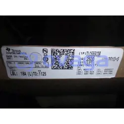
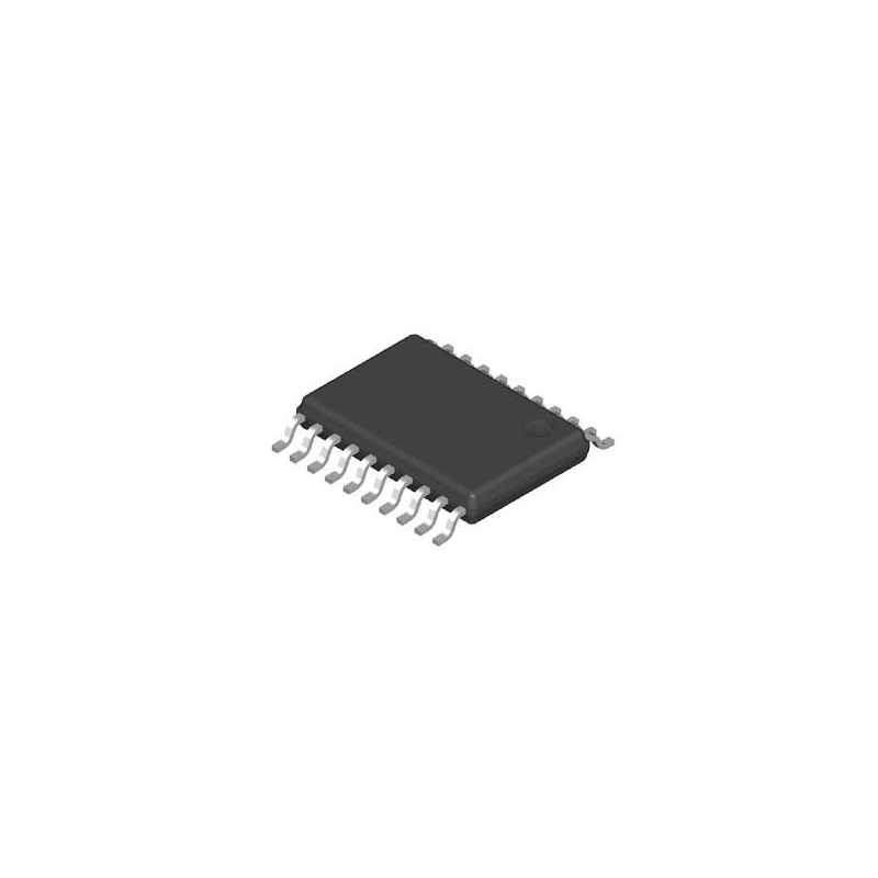
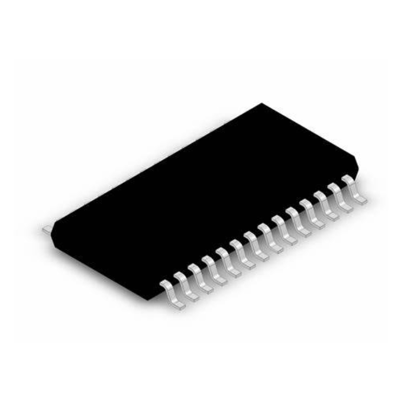
$50005T93GL06NLGI
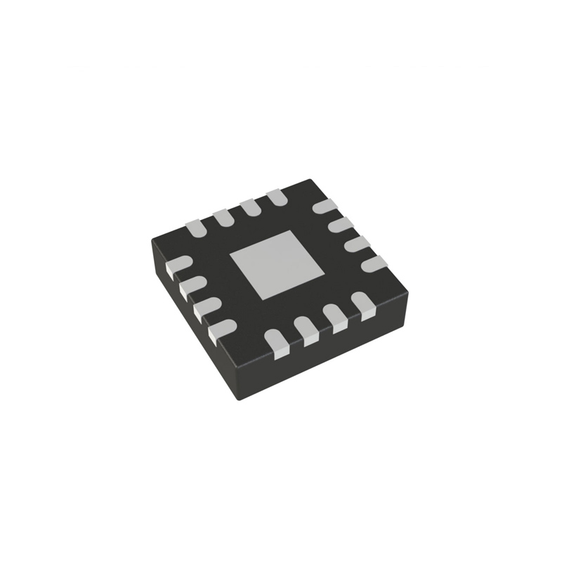
Clock Fanout Buffer (Distribution), Multiplexer IC 2:6 800 MHz 28-VQFN Exposed Pad


5T93GL06NLGI 일반적인 설명
The 5T93GL06 2.5V differential clock buffer is a user- selectable differential input to six LVDS outputs. The fanout from a differential input to six LVDS outputs reduces loading on the preceding driver and provides an efficient clock distribution network. The 5T93GL06 can act as a translator from a differential HSTL, eHSTL, LVEPECL (2.5V), LVPECL (3.3V), CML, or LVDS input to LVDS outputs. A single-ended 3.3V / 2.5V LVTTL input can also be used to translate to LVDS outputs. The redundant input capability allows for a glitchless change-over from a primary clock source to a secondary clock source up to 650MHz. Selectable inputs are controlled by SEL. During the switchover, the output will disable low for up to three clock cycles of the previously-selected input clock. The outputs will remain low for up to three clock cycles of the newly-selected clock, after which the outputs will start from the newly-selected input. A FSEL pin has been implemented to control the switchover in cases where a clock source is absent or is driven to DC levels below the minimum specifications. The 5T93GL06 outputs can be asynchronously enabled/ disabled. When disabled, the outputs will drive to the value selected by the GL pin. Multiple power and grounds reduce noise.
특징
- Guaranteed low skew: <25ps (maximum)
- Very low duty cycle distortion: <100ps (maximum)
- High speed propagation delay: <2ns (maximum)
- Up to 800MHz operation
- Glitchless input clock switching up to 650MHz
- Selectable inputs
- Hot insertable and over-voltage tolerant inputs
- 3.3V/2.5V LVTTL, HSTL, eHSTL, LVEPECL (2.5V), LVPECL (3.3V), CML or LVDS input interface
- Selectable differential inputs to six LVDS outputs
- Power-down mode
- At power-up, FSEL should be LOW
- 2.5V VDD
- -40°C to 85°C ambient operating temperature
- Available in VFQFN package
- Recommends IDT5T9306 if glitchless input selection is not required
명세서
| 매개변수 | 값 | 매개변수 | 값 |
|---|---|---|---|
| Pkg. Type | VFQFPN | Lead Count (#) | 28 |
| Temp. Grade | I | Pb (Lead) Free | Yes |
| Carrier Type | Tray |
배송
| 배송 유형 | 배송비 | 리드타임 | |
|---|---|---|---|
 |
DHL | $20.00-$40.00 (0.50 KG) | 2-5 날 |
 |
페덱스 | $20.00-$40.00 (0.50 KG) | 2-5 날 |
 |
UPS | $20.00-$40.00 (0.50 KG) | 2-5 날 |
 |
TNT | $20.00-$40.00 (0.50 KG) | 2-5 날 |
 |
EMS | $20.00-$40.00 (0.50 KG) | 2-5 날 |
 |
등기 항공 우편 | $20.00-$40.00 (0.50 KG) | 2-5 날 |
처리 시간: 배송비는 지역 및 국가에 따라 다릅니다.
지불
| 지불 조건 | 핸드 수수료 | |
|---|---|---|
 |
은행 송금 | US$30.00의 은행 수수료를 부과합니다. |
 |
페이팔 | 4.0%의 서비스 수수료를 부과합니다. |
 |
신용 카드 | 3.5% 서비스 수수료를 부과합니다. |
 |
웨스턴 유니언 | charge US.00 banking fee. |
 |
돈 그램 | US$0.00의 은행 수수료를 부과합니다. |
보증
1. 귀하가 구입한 전자 부품에는 365일 보증이 포함되어 있으며, 우리는 제품 품질을 보장합니다.
2. 귀하가 받은 품목 중 일부가 완벽한 품질이 아닌 경우, 당사는 책임 있게 귀하의 환불 또는 교체를 준비할 것입니다. 그러나 품목은 원래 상태를 유지해야 합니다.
포장
-

단계1 :제품
-

단계2 :진공 포장
-

단계3 :정전기 방지 가방
-

단계4 :개별 포장
-

단계5 :포장 상자
-

단계6 :바코드 배송 태그


모든 제품은 정전기 방지 가방에 포장됩니다. ESD 정전기 방지 보호 장치와 함께 배송됩니다.
외부 ESD 포장 라벨은 당사 정보(부품 번호, 브랜드 및 수량)를 사용합니다.
우리는 선적 전에 모든 상품을 검사하고, 모든 제품이 양호한 상태인지 확인하고, 부품이 새로운 원본 일치 데이터시트인지 확인합니다.
모든 상품을 포장한 후 문제가 없는지 확인한 후 안전하게 포장하여 글로벌 특급으로 보내드립니다. 우수한 밀봉 무결성과 함께 탁월한 천공 및 인열 저항성을 나타냅니다.


우리는 고품질 제품, 사려 깊은 서비스 및 판매 후 보증을 제공합니다.
-

우리는 풍부한 제품을 보유하고 있으며 귀하의 다양한 요구를 충족시킬 수 있습니다.
-

최소 주문 수량은 1개부터입니다.
-

최저 국제 배송비는 $0.00부터 시작됩니다
-

모든 제품에 대해 365일 품질 보증