

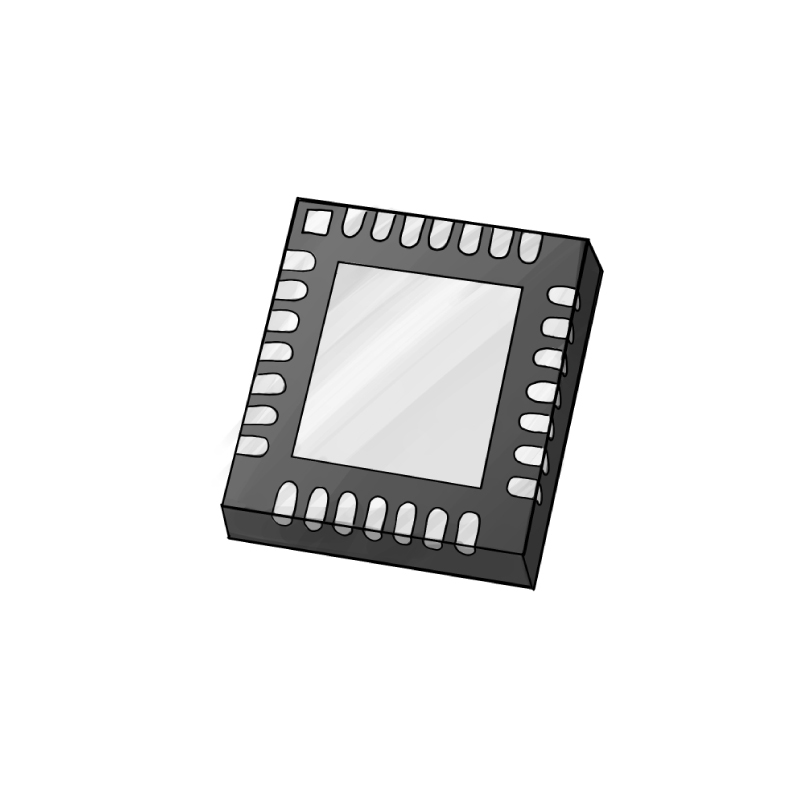
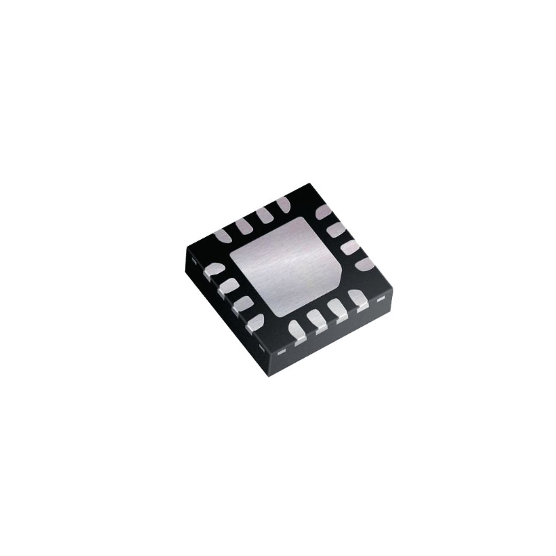
이미지는 참고용입니다. 제품 사양 보기
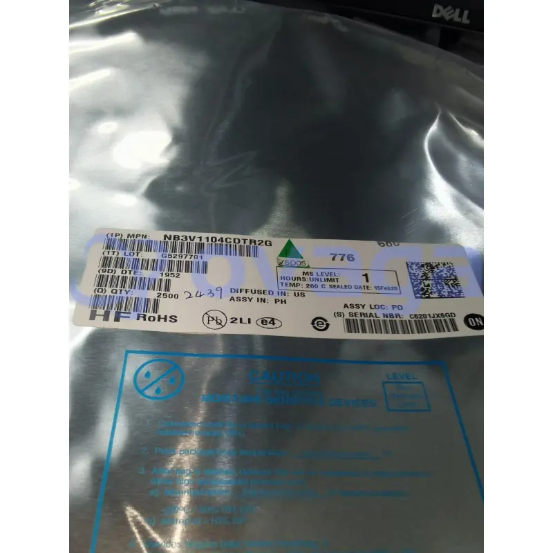
ON NB3V1104CDTR2G

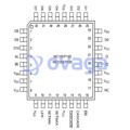
Clock Fanout Buffer (Distribution) IC 1:4 250 MHz 8-TSSOP (0.173", 4.40mm Width)


제조업체부품 #: NB3V1104CDTR2G
데이터 시트: NB3V1104CDTR2G Datasheet (PDF)
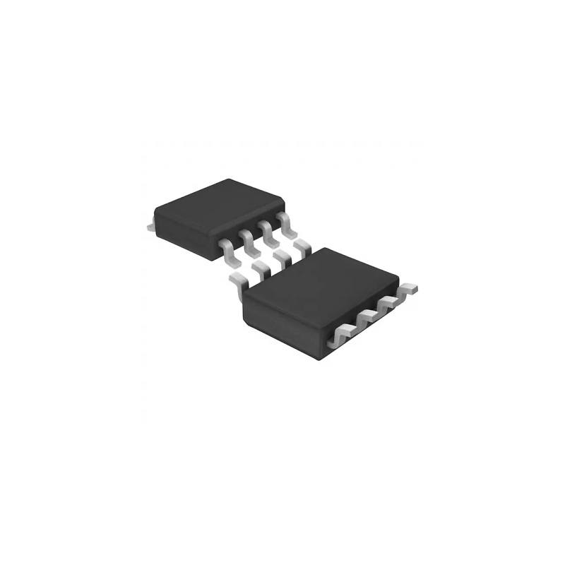
패키지/케이스: TSSOP-8
RoHS 상태:
재고상태: 2167 PC, 새로운 원본
상품 유형: 시계 및 타이머 IC
Warranty: 1 Year Ovaga Warranty - Find Out More
0
1
*모든 가격은 USD 단위입니다.
| 수량 | 단가 | 추가 가격 |
|---|---|---|
| 1 | $2.267 | $2.267 |
| 10 | $1.960 | $19.600 |
| 30 | $1.768 | $53.040 |
| 100 | $1.572 | $157.200 |
| 500 | $1.483 | $741.500 |
| 1000 | $1.444 | $1444.000 |
In Stock:2167 PCS
NB3V1104CDTR2G 일반적인 설명
The NB3V1104C is a member of the NB3V110xC a modular, high−performance, low−skew, general purpose LVCMOS clock buffer family. The device has a 1:4 fan-out. The family of devices is designed with a modular approach. Different fan-out variations, 1:2, 1:3, 1:4, 1:6 and 1:8, are available. All of the devices are pin compatible to each other for easy handling. All family members share the same high performing characteristics like low additive jitter, low skew, and wide operating temperature range. The NB3V110xCsupports an asynchronous output enable control (OE) which switchesthe outputs into a low state when OE is low. The NB3V110xC operatein a 3.3 V, 2.5 V and 1.8 V environment and are characterized for operation from –40°C to 105°C.
특징
- High−Performance 1:4 LVCMOS Clock Buffer
- Very Low Output−to−Output Skew < 50 ps
- Supply Voltage: 3.3 V, 2.5 V or 1.8 V
- Available in 8−Pin TSSOP
- Operating Temperature Range: –40°C to 105°C
- Low Additive Jitter
- fmax = 250 MHz for 3.3 V; fmax = 180 MHz for 2.5 V; fmax = 133 MHz for 1.8 V
- These Devices are Pb−Free and are RoHS Compliant
애플리케이션
- Clock Distribution
- Networking and Data Communication
- High-end Computing
명세서
| 매개변수 | 값 | 매개변수 | 값 |
|---|---|---|---|
| Manufacturer: | ON Semiconductor | Product Category: | Clock Buffer |
| RoHS: | Y | Series: | NB3V110xC |
| Packaging: | Reel | Brand: | ON Semiconductor |
| Product Type: | Clock Buffer | Factory Pack Quantity: | 2500 |
| Subcategory: | Clock & Timer ICs | Tags | NB3V1, NB3V, NB3 |
| Source Content uid | NB3V1104CDTR2G | Pbfree Code | Yes |
| Part Life Cycle Code | Active | Ihs Manufacturer | ONSEMI |
| Package Description | TSSOP-14 | Manufacturer Package Code | 948S-01 |
| Reach Compliance Code | compliant | HTS Code | 8542.39.00.01 |
| Factory Lead Time | 71 Weeks | Samacsys Manufacturer | onsemi |
| Additional Feature | ALSO OPERATES AT 2.5V AND 3.3V VCC NOMINAL SUPPLY | Family | NB3V |
| Input Conditioning | STANDARD | JESD-30 Code | R-PDSO-G14 |
| Logic IC Type | LOW SKEW CLOCK DRIVER | Moisture Sensitivity Level | 1 |
| Number of Functions | 1 | Number of Inverted Outputs | |
| Number of Terminals | 14 | Number of True Outputs | 4 |
| Output Characteristics | 3-STATE | Package Body Material | PLASTIC/EPOXY |
| Package Code | TSSOP | Package Shape | RECTANGULAR |
| Package Style | SMALL OUTLINE, THIN PROFILE, SHRINK PITCH | Packing Method | TR |
| Peak Reflow Temperature (Cel) | 260 | Surface Mount | YES |
| Temperature Grade | INDUSTRIAL | Terminal Finish | NICKEL PALLADIUM GOLD |
| Terminal Form | GULL WING | Terminal Position | DUAL |
| Time@Peak Reflow Temperature-Max (s) | 30 |
배송
| 배송 유형 | 배송비 | 리드타임 | |
|---|---|---|---|
 |
DHL | $20.00-$40.00 (0.50 KG) | 2-5 날 |
 |
페덱스 | $20.00-$40.00 (0.50 KG) | 2-5 날 |
 |
UPS | $20.00-$40.00 (0.50 KG) | 2-5 날 |
 |
TNT | $20.00-$40.00 (0.50 KG) | 2-5 날 |
 |
EMS | $20.00-$40.00 (0.50 KG) | 2-5 날 |
 |
등기 항공 우편 | $20.00-$40.00 (0.50 KG) | 2-5 날 |
처리 시간: 배송비는 지역 및 국가에 따라 다릅니다.
지불
| 지불 조건 | 핸드 수수료 | |
|---|---|---|
 |
은행 송금 | US$30.00의 은행 수수료를 부과합니다. |
 |
페이팔 | 4.0%의 서비스 수수료를 부과합니다. |
 |
신용 카드 | 3.5% 서비스 수수료를 부과합니다. |
 |
웨스턴 유니언 | charge US.00 banking fee. |
 |
돈 그램 | US$0.00의 은행 수수료를 부과합니다. |
보증
1. 귀하가 구입한 전자 부품에는 365일 보증이 포함되어 있으며, 우리는 제품 품질을 보장합니다.
2. 귀하가 받은 품목 중 일부가 완벽한 품질이 아닌 경우, 당사는 책임 있게 귀하의 환불 또는 교체를 준비할 것입니다. 그러나 품목은 원래 상태를 유지해야 합니다.
포장
-

단계1 :제품
-

단계2 :진공 포장
-

단계3 :정전기 방지 가방
-

단계4 :개별 포장
-

단계5 :포장 상자
-

단계6 :바코드 배송 태그


모든 제품은 정전기 방지 가방에 포장됩니다. ESD 정전기 방지 보호 장치와 함께 배송됩니다.
외부 ESD 포장 라벨은 당사 정보(부품 번호, 브랜드 및 수량)를 사용합니다.
우리는 선적 전에 모든 상품을 검사하고, 모든 제품이 양호한 상태인지 확인하고, 부품이 새로운 원본 일치 데이터시트인지 확인합니다.
모든 상품을 포장한 후 문제가 없는지 확인한 후 안전하게 포장하여 글로벌 특급으로 보내드립니다. 우수한 밀봉 무결성과 함께 탁월한 천공 및 인열 저항성을 나타냅니다.


부품 포인트
-
The NB3V1104CDTR2G chip is a voltage controlled oscillator (VCO) designed for low phase noise applications. It operates at a frequency range of 150MHz to 190MHz and provides an output in the form of a square wave. This chip is commonly used in communication systems, radio frequency (RF) equipment, and wireless devices to generate stable and accurate clock signals.
-
Features
Features of NB3V1104CDTR2G include a low power consumption of 3 µA, a wide voltage supply range of 1.65V to 5.5V, a compact size of 1.2 x 1.2 mm, a wide temperature range of -40°C to +85°C, and a stable operation with low jitter. It also offers a 2.5V compatibility and supports I2C interface. -
Pinout
The NB3V1104CDTR2G is a 1:4 clock buffer with a pin count of 16. Its functions include voltage level translation, clock distribution, and clock signal buffering for various applications. -
Manufacturer
The manufacturer of the NB3V1104CDTR2G is ON Semiconductor. ON Semiconductor is a multinational semiconductor manufacturing company that specializes in a wide range of products, including power management, signal conditioning, custom devices, and standard components. They provide innovative solutions for various industries, including automotive, industrial, communication, and consumer electronics. -
Application Field
The NB3V1104CDTR2G is a high-speed clock and data recovery IC designed for applications that require data transfer over long distances. It is commonly used in optical communication systems, fiber-optic networks, and high-speed data transmission applications in telecommunications and networking. -
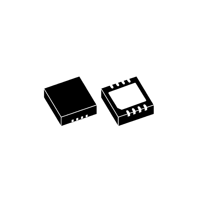
Package
The NB3V1104CDTR2G chip is available in a package type called DFN-6 (Dual Flat No-Lead). It has a form factor of 3mm x 3mm and a size of approximately 15.4mm².

데이터 시트 PDF
우리는 고품질 제품, 사려 깊은 서비스 및 판매 후 보증을 제공합니다.
-

우리는 풍부한 제품을 보유하고 있으며 귀하의 다양한 요구를 충족시킬 수 있습니다.
-

최소 주문 수량은 1개부터입니다.
-

최저 국제 배송비는 $0.00부터 시작됩니다
-

모든 제품에 대해 365일 품질 보증


평가 및 리뷰
Ovaga's website is easy to use and their selection of electronic components is unparalleled.


Average products, but quick shipping.