이미지는 참고용입니다. 제품 사양 보기
주문 금액이
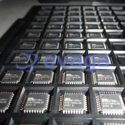
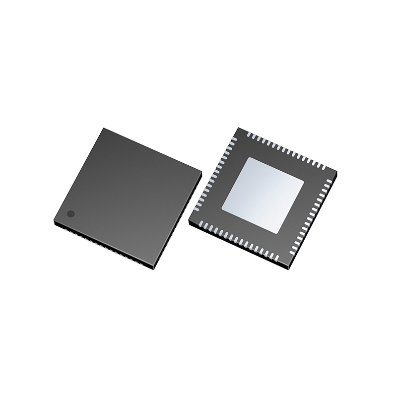
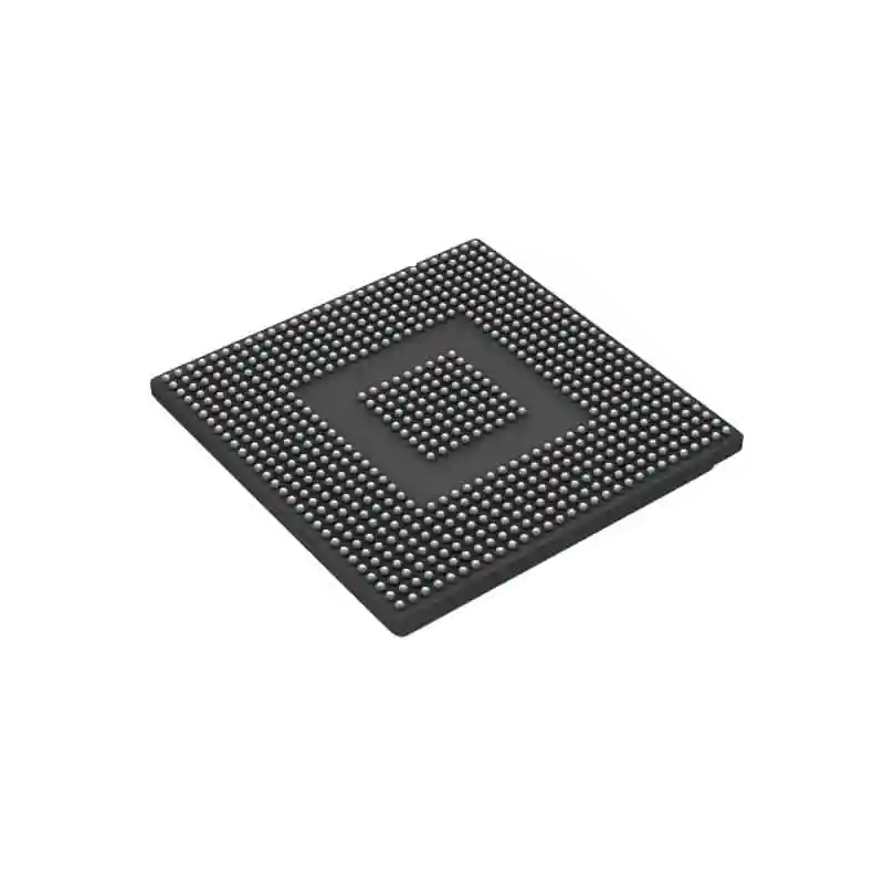
$5000Microchip ZL30663LFG7
Clock Generators & Support Products Triple channel SyncE Line Card


ZL30663LFG7 일반적인 설명
The ZL30663 offers three channels of Synchronous Ethernet (SyncE) packet clock synchronization. Using Microsemi’s miTimePLL timing technology, this device offers new and improved features for 5G transport and wireless infrastructure equipment. Each device integrates all features required by line card PLL. High integration along with ultra-low jitter make these devices ideal for use in frequency translation from backplane clock to frequencies required by PHY devices, jitter filtering, and holdover in case both active and redundant timing cards fail.
Under the same family, the ZL3069x offer one to three channels of Synchronous Ethernet (SyncE) packet clock synchronization for timing card interface. Also available is ZL3079x that support one to three independent timing channels of a combined hardware and software platform including IEEE 1588-2008 Precision Time Protocol Stack and Synchronization Algorithms.
Log in to your MyMicrochip account (with SDE enabled) and request for data sheet and the following application notes.
AN3467 Crystals and Oscillators for Next Generation Timing Solutions
ZLAN-649 ZL3067x Power Supply Decoupling and Layout Practices
ZLAN-656 Redwood PSNR
ZLAN-664 Board Design Recommendations for Redwood
ZLAN-672 Generating JESD204B Clock SYSREF Using Redwood
ZLAN-683 Assembly and PCB Layout Guidelines for 80-lead LGA Package
ZLAN-724 Phase Measurement Compensation for Redwood
ZLAN-728 Indirect Read and Write Procedure
특징
- Three independent DPLL channels
- Precise phase/frequency measurement and tuning lower system latency to meet 4G LTE, 5G & Wireless Infrastructure
- Precise chip-to-chip time interfaces use less backplane traces for 1PPS distribution for chassis systems
- Split oscillator option lowers cost, lowers jitter, and provides redundancy
- Excellent jitter performance of <300 fs RMS in the 12 kHz to 20 MHz band meets jitter requirements for 10G/40G and 100G PHYs
- Two programmable ultra-low jitter synthesizers generate any frequency from 0.5 Hz to 1045 MHz
- One programmable general purpose synthesizer generates any clock from 0.5 Hz to 180 MHz
- Programmable output advancement/delay to accommodate trace delays or compensate for system routing paths
- 8 differential or 16 single ended ultra-low jitter outputs plus two general purpose CMOS outputs
- Up to three programmable digital PLLs/NCOs with loop bandwidth from 14 Hz to 470 Hz synchronize to any clock rate from 0.5 Hz to 900 MHz
- Accepts up to 10 differential or 10 single ended input references
- Full reference monitoring of electrical failures
- Automatic hitless reference switching and digital holdover on reference fail with initial holdover accuracy better than 0.1 ppb
- Any input reference can be fed with clock, sync (frame pulse), clock /sync pair or clock modulated with sync pulse (embedded PPS ePPS and embedded PP2S ePP2S)
- Easy Configuration and dynamic programming via SPI/I2C interface
- Factory programming available
- Operates from a single crystal resonator or clock oscillator
- Line card timing function for carrier network equipment compliant to ITU-T G.8262, G.8273.2, G.8273.4
- Communications systems timed by any combination of Synchronous Ethernet, IEEE 1588 PTP, or GPS/GNSS
- 5G wireless CU, DU, and RU systems
- 5G systems with precise time requirements driven by advanced services such as carrier aggregation, coordinated multipoint, OTDOA location, etc.
- Carrier routers, access aggregation, wireless backhaul,
- SONET/SDH systems
- Applications/Uses
명세서
| 매개변수 | 값 | 매개변수 | 값 |
|---|---|---|---|
| Manufacturer | Microchip | Product Category | Clock Generators & Support Products |
| RoHS | Details | Type | Clock Synchronizers |
| Maximum Input Frequency | 900 MHz | Max Output Freq | 1.045 GHz |
| Number of Outputs | 10 Output | Duty Cycle - Max | - |
| Operating Supply Voltage | 1.8 V, 3.3 V | Minimum Operating Temperature | - 40 C |
| Maximum Operating Temperature | + 85 C | Mounting Style | SMD/SMT |
| Brand | Microchip Technology | Product Type | Clock Generators |
| Factory Pack Quantity | 176 |
배송
| 배송 유형 | 배송비 | 리드타임 | |
|---|---|---|---|
 |
DHL | $20.00-$40.00 (0.50 KG) | 2-5 날 |
 |
페덱스 | $20.00-$40.00 (0.50 KG) | 2-5 날 |
 |
UPS | $20.00-$40.00 (0.50 KG) | 2-5 날 |
 |
TNT | $20.00-$40.00 (0.50 KG) | 2-5 날 |
 |
EMS | $20.00-$40.00 (0.50 KG) | 2-5 날 |
 |
등기 항공 우편 | $20.00-$40.00 (0.50 KG) | 2-5 날 |
처리 시간: 배송비는 지역 및 국가에 따라 다릅니다.
지불
| 지불 조건 | 핸드 수수료 | |
|---|---|---|
 |
은행 송금 | US$30.00의 은행 수수료를 부과합니다. |
 |
페이팔 | 4.0%의 서비스 수수료를 부과합니다. |
 |
신용 카드 | 3.5% 서비스 수수료를 부과합니다. |
 |
웨스턴 유니언 | charge US.00 banking fee. |
 |
돈 그램 | US$0.00의 은행 수수료를 부과합니다. |
보증
1. 귀하가 구입한 전자 부품에는 365일 보증이 포함되어 있으며, 우리는 제품 품질을 보장합니다.
2. 귀하가 받은 품목 중 일부가 완벽한 품질이 아닌 경우, 당사는 책임 있게 귀하의 환불 또는 교체를 준비할 것입니다. 그러나 품목은 원래 상태를 유지해야 합니다.
포장
-

단계1 :제품
-

단계2 :진공 포장
-

단계3 :정전기 방지 가방
-

단계4 :개별 포장
-

단계5 :포장 상자
-

단계6 :바코드 배송 태그


모든 제품은 정전기 방지 가방에 포장됩니다. ESD 정전기 방지 보호 장치와 함께 배송됩니다.
외부 ESD 포장 라벨은 당사 정보(부품 번호, 브랜드 및 수량)를 사용합니다.
우리는 선적 전에 모든 상품을 검사하고, 모든 제품이 양호한 상태인지 확인하고, 부품이 새로운 원본 일치 데이터시트인지 확인합니다.
모든 상품을 포장한 후 문제가 없는지 확인한 후 안전하게 포장하여 글로벌 특급으로 보내드립니다. 우수한 밀봉 무결성과 함께 탁월한 천공 및 인열 저항성을 나타냅니다.


우리는 고품질 제품, 사려 깊은 서비스 및 판매 후 보증을 제공합니다.
-

우리는 풍부한 제품을 보유하고 있으며 귀하의 다양한 요구를 충족시킬 수 있습니다.
-

최소 주문 수량은 1개부터입니다.
-

최저 국제 배송비는 $0.00부터 시작됩니다
-

모든 제품에 대해 365일 품질 보증