이미지는 참고용입니다. 제품 사양 보기
주문 금액이
$5000XPC850DSLZT50BU
The XPC850DSLZT50BU is a cutting-edge RISC microprocessor with 32-bit architecture, ideal for fast data processing


브랜드: NXP USA Inc.
제조업체부품 #: XPC850DSLZT50BU
데이터 시트: XPC850DSLZT50BU 데이터 시트 (PDF)
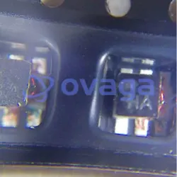
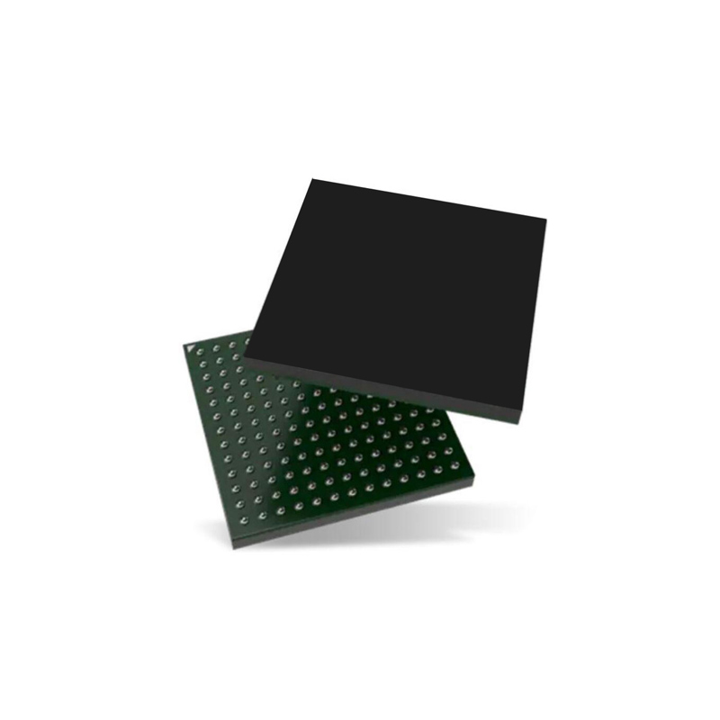
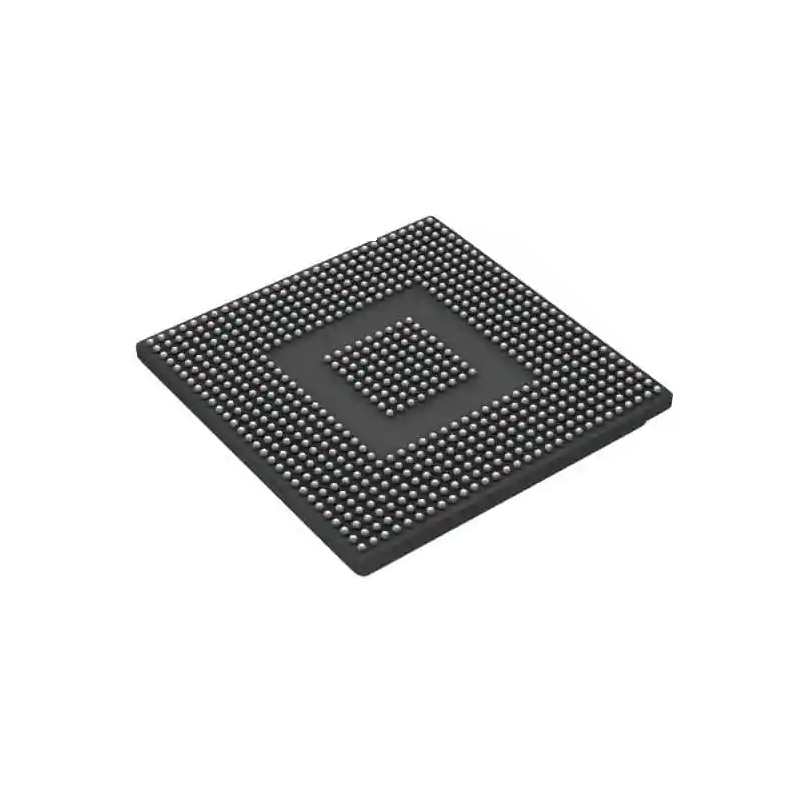
패키지/케이스: 256-BGA
상품 유형: Microprocessors
XPC850DSLZT50BU 일반적인 설명
The XPC850DSLZT50BU microprocessor from Freescale Semiconductor stands out as a PowerQUICC chip designed for embedded systems that demand a blend of performance and power efficiency. Operating at a clock speed of 50 MHz, this processor strikes a balance that caters to applications requiring moderate processing power. Its incorporation of peripherals like UARTs, timers, and I/O interfaces offers system designers a versatile platform for crafting tailored solutions. The 'DSL' indication within the product code signifies support for DDR SDRAM interfaces, providing a boost to memory bandwidth and enhancing data processing speeds. On the other hand, the 'ZT' likely represents unique features or variations that differentiate this microprocessor within its product lineup
특징
The following list summarizes the key MPC860 features:
Embedded single-issue, 32-bit MPC8xx core (implementing the PowerPC architecture) with thirty-two 32-bit general-purpose registers (GPRs)
The core performs branch prediction with conditional prefetch, without conditional execution
4- or 8-Kbyte data cache and 4- or 16-Kbyte instruction cache (see Table 1)
16-Kbyte instruction caches are four-way, set-associative with 256 sets;
4-Kbyte instruction caches are two-way, set-associative with 128 sets.
8-Kbyte data caches are two-way, set-associative with 256 sets; 4-Kbyte data caches are two-way, set-associative with 128 sets.
Cache coherency for both instruction and data caches is maintained on 128-bit (4-word) cache blocks.
Caches are physically addressed, implement a least recently used (LRU) replacement algorithm, and are lockable on a cache block basis.
Instruction and data caches are two-way, set-associative, physically addressed, LRU replacement, and lockable on-line granularity.
MMUs with 32-entry TLB, fully associative instruction, and data TLBs
MMUs support multiple page sizes of 4, 16, and 512 Kbytes, and 8 Mbytes; 16 virtual address spaces and 16 protection groups
Advanced on-chip-emulation debug mode
Up to 32-bit data bus (dynamic bus sizing for 8, 16, and 32 bits)
32 address lines
Operates at up to 80 MHz
Memory controller (eight banks)
Contains complete dynamic RAM (DRAM) controller
Each bank can be a chip select or RASto support a DRAM bank
Up to 15 wait states programmable per memory bank
Glueless interface to DRAM, SIMMS, SRAM, EPROM, Flash EPROM, and other memory devices.
DRAM controller programmable to support most size and speed memory interfaces
Four CASlines, four WElines, one OEline
Boot chip-select available at reset (options for 8-, 16-, or 32-bit memory)
Variable block sizes (32 Kbyte to 256 Mbyte)
Selectable write protection
On-chip bus arbitration logic
General-purpose timers
Four 16-bit timers or two 32-bit timers
Gate mode can enable/disable counting
Interrupt can be masked on reference match and event capture
System integration unit (SIU)
Bus monitor
Software watchdog
Periodic interrupt timer (PIT)
Low-power stop mode
Clock synthesizer
Three parallel I/O registers with open-drain capability
Four baud-rate generators (BRGs)
Independent (can be connected to any SCC or SMC)
Allow changes during operation
Autobaud support option
Four serial communications controllers (SCCs)
Ethernet/IEEE 802.3 optional on SCC14, supporting full 10-Mbps operation (available only on specially programmed devices).
HDLC/SDLC(all channels supported at 2 Mbps)
HDLC bus (implements an HDLC-based local area network (LAN))
Asynchronous HDLC to support PPP (point-to-point protocol)
AppleTalk
Universal asynchronous receiver transmitter (UART)
Synchronous UART
Serial infrared (IrDA)
Binary synchronous communication (BISYNC)
Totally transparent (bit streams)
Totally transparent (frame based with optional cyclic redundancy check (CRC))
Two SMCs (serial management channels)
UART
Transparent
General circuit interface (GCI) controller
Can be connected to the time-division multiplexed (TDM) channels
One SPI (serial peripheral interface)
Supports master and slave modes
Supports multimaster operation on the same bus
One I2C (inter-integrated circuit) port
Supports master and slave modes
Multiple-master environment support
Time-slot assigner (TSA)
Allows SCCs and SMCs to run in multiplexed and/or non-multiplexed operation
Supports T1, CEPT, PCM highway, ISDN basic rate, ISDN primary rate, user defined
1- or 8-bit resolution
Allows independent transmit and receive routing, frame synchronization, clocking
Allows dynamic changes
Can be internally connected to six serial channels (four SCCs and two SMCs)
Parallel interface port (PIP)
Centronics interface support
Supports fast connection between compatible ports on the MPC860 or the MC68360
PCMCIA interface
Master (socket) interface, release 2.1 compliant
Supports two independent PCMCIA sockets
Eight memory or I/O windows supported
Low power support
Full onall units fully powered
Dozecore functional units disabled, except time base decrementer, PLL, memory controller, RTC, and CPM in low-power standby
Sleepall units disabled, except RTC and PIT, PLL active for fast wake up
Deep sleepall units disabled including PLL, except RTC and PIT
Power down mode all units powered down, except PLL, RTC, PIT, time base, and decrementer
Debug interface
Eight comparators: four operate on instruction address, two operate on data address, and two operate on data
Supports conditions: =<>
Each watchpoint can generate a break-point internally
3.3 V operation with 5-V TTL compatibility except EXTAL and EXTCLK
357-pin ball grid array (BGA) package
명세서
| 매개변수 | 값 | 매개변수 | 값 |
|---|---|---|---|
| Series | MPC8xx | Package | Tray |
| Product Status | Obsolete | Core Processor | MPC8xx |
| Number of Cores/Bus Width | 1 Core, 32-Bit | Speed | 50MHz |
| Co-Processors/DSP | Communications; CPM | RAM Controllers | DRAM |
| Graphics Acceleration | No | Ethernet | 10Mbps (1) |
| USB | USB 1.x (1) | Voltage - I/O | 3.3V |
| Operating Temperature | 0°C ~ 95°C (TA) | Mounting Type | Surface Mount |
| Package / Case | 256-BGA | Supplier Device Package | 256-PBGA (23x23) |
| Additional Interfaces | HDLC/SDLC, I2C, IrDA, PCMCIA-ATA, TDM, UART/USART |
배송
| 배송 유형 | 배송비 | 리드타임 | |
|---|---|---|---|
 |
DHL | $20.00-$40.00 (0.50 KG) | 2-5 날 |
 |
페덱스 | $20.00-$40.00 (0.50 KG) | 2-5 날 |
 |
UPS | $20.00-$40.00 (0.50 KG) | 2-5 날 |
 |
TNT | $20.00-$40.00 (0.50 KG) | 2-5 날 |
 |
EMS | $20.00-$40.00 (0.50 KG) | 2-5 날 |
 |
등기 항공 우편 | $20.00-$40.00 (0.50 KG) | 2-5 날 |
처리 시간: 배송비는 지역 및 국가에 따라 다릅니다.
지불
| 지불 조건 | 핸드 수수료 | |
|---|---|---|
 |
은행 송금 | US$30.00의 은행 수수료를 부과합니다. |
 |
페이팔 | 4.0%의 서비스 수수료를 부과합니다. |
 |
신용 카드 | 3.5% 서비스 수수료를 부과합니다. |
 |
웨스턴 유니언 | charge US.00 banking fee. |
 |
돈 그램 | US$0.00의 은행 수수료를 부과합니다. |
보증
1. 귀하가 구입한 전자 부품에는 365일 보증이 포함되어 있으며, 우리는 제품 품질을 보장합니다.
2. 귀하가 받은 품목 중 일부가 완벽한 품질이 아닌 경우, 당사는 책임 있게 귀하의 환불 또는 교체를 준비할 것입니다. 그러나 품목은 원래 상태를 유지해야 합니다.
포장
-

단계1 :제품
-

단계2 :진공 포장
-

단계3 :정전기 방지 가방
-

단계4 :개별 포장
-

단계5 :포장 상자
-

단계6 :바코드 배송 태그


모든 제품은 정전기 방지 가방에 포장됩니다. ESD 정전기 방지 보호 장치와 함께 배송됩니다.
외부 ESD 포장 라벨은 당사 정보(부품 번호, 브랜드 및 수량)를 사용합니다.
우리는 선적 전에 모든 상품을 검사하고, 모든 제품이 양호한 상태인지 확인하고, 부품이 새로운 원본 일치 데이터시트인지 확인합니다.
모든 상품을 포장한 후 문제가 없는지 확인한 후 안전하게 포장하여 글로벌 특급으로 보내드립니다. 우수한 밀봉 무결성과 함께 탁월한 천공 및 인열 저항성을 나타냅니다.


우리는 고품질 제품, 사려 깊은 서비스 및 판매 후 보증을 제공합니다.
-

우리는 풍부한 제품을 보유하고 있으며 귀하의 다양한 요구를 충족시킬 수 있습니다.
-

최소 주문 수량은 1개부터입니다.
-

최저 국제 배송비는 $0.00부터 시작됩니다
-

모든 제품에 대해 365일 품질 보증