

이미지는 참고용입니다. 제품 사양 보기
주문 금액이
$5000
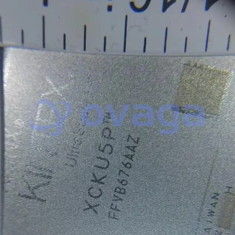
Xilinx XCKU5P-2FFVB676I

Kintex® UltraScale+™ Field Programmable Gate Array (FPGA) IC 280 41984000 474600 676-BBGA, FCBGA


브랜드: AMD Xilinx, Inc
제조업체부품 #: XCKU5P-2FFVB676I
데이터 시트: XCKU5P-2FFVB676I Datasheet (PDF)
패키지/케이스: FBGA-676
RoHS 상태:
재고상태: 3,844 PC, 새로운 원본
상품 유형: FPGAs (Field Programmable Gate Array)
Warranty: 1 Year Ovaga Warranty - Find Out More
0
1
*모든 가격은 USD 단위입니다.
| 수량 | 단가 | 추가 가격 |
|---|---|---|
| 1 | $183.108 | $183.108 |
| 30 | $175.304 | $5259.120 |
재고: 3,844 PCS
XCKU5P-2FFVB676I 일반적인 설명
Kintex® UltraScale+™ Field Programmable Gate Array (FPGA) IC 280 41984000 474600 676-BBGA, FCBGA
특징
IC FPGA 280 I/O 676FCBGAIC FPGA 280 I/O 676FCBGA
명세서
| 매개변수 | 값 | 매개변수 | 값 |
|---|---|---|---|
| Pin Count | 676 | Package Category | BGA |
| Released Date | Jul 28, 2020 |
배송
| 배송 유형 | 배송비 | 리드타임 | |
|---|---|---|---|
 |
DHL | $20.00-$40.00 (0.50 KG) | 2-5 날 |
 |
페덱스 | $20.00-$40.00 (0.50 KG) | 2-5 날 |
 |
UPS | $20.00-$40.00 (0.50 KG) | 2-5 날 |
 |
TNT | $20.00-$40.00 (0.50 KG) | 2-5 날 |
 |
EMS | $20.00-$40.00 (0.50 KG) | 2-5 날 |
 |
등기 항공 우편 | $20.00-$40.00 (0.50 KG) | 2-5 날 |
처리 시간: 배송비는 지역 및 국가에 따라 다릅니다.
지불
| 지불 조건 | 핸드 수수료 | |
|---|---|---|
 |
은행 송금 | US$30.00의 은행 수수료를 부과합니다. |
 |
페이팔 | 4.0%의 서비스 수수료를 부과합니다. |
 |
신용 카드 | 3.5% 서비스 수수료를 부과합니다. |
 |
웨스턴 유니언 | charge US.00 banking fee. |
 |
돈 그램 | US$0.00의 은행 수수료를 부과합니다. |
보증
1. 귀하가 구입한 전자 부품에는 365일 보증이 포함되어 있으며, 우리는 제품 품질을 보장합니다.
2. 귀하가 받은 품목 중 일부가 완벽한 품질이 아닌 경우, 당사는 책임 있게 귀하의 환불 또는 교체를 준비할 것입니다. 그러나 품목은 원래 상태를 유지해야 합니다.
포장
-

단계1 :제품
-

단계2 :진공 포장
-

단계3 :정전기 방지 가방
-

단계4 :개별 포장
-

단계5 :포장 상자
-

단계6 :바코드 배송 태그


모든 제품은 정전기 방지 가방에 포장됩니다. ESD 정전기 방지 보호 장치와 함께 배송됩니다.
외부 ESD 포장 라벨은 당사 정보(부품 번호, 브랜드 및 수량)를 사용합니다.
우리는 선적 전에 모든 상품을 검사하고, 모든 제품이 양호한 상태인지 확인하고, 부품이 새로운 원본 일치 데이터시트인지 확인합니다.
모든 상품을 포장한 후 문제가 없는지 확인한 후 안전하게 포장하여 글로벌 특급으로 보내드립니다. 우수한 밀봉 무결성과 함께 탁월한 천공 및 인열 저항성을 나타냅니다.


부품 포인트
-
The XCKU5P-2FFVB676I chip is a Field-Programmable Gate Array (FPGA) by Xilinx. It is part of the Kintex UltraScale+ family and features advanced capabilities such as high-performance processing and integration of system-level functions. The chip offers a large number of programmable logic cells, I/O capabilities, and additional resources for various applications in industries like aerospace, telecommunications, and automotive.
-
Equivalent
There are no direct equivalent products to the XCKU5P-2FFVB676I chip. However, it belongs to the Xilinx Kintex Ultrascale+ family of FPGAs, and other members of this family, such as XCKU5P-2FFVA676I and XCKU5P-1FFVA1156I, may offer similar functionality. -
Features
XCKU5P-2FFVB676I is a programmable FPGA device. It features a high-performance Kintex UltraScale architecture with 915,000 logic cells and 1,728 DSP slices, designed for applications requiring high processing bandwidth and low power consumption. It also offers a range of I/O options, including PCI Express and Ethernet interfaces. -
Pinout
The XCKU5P-2FFVB676I is a field-programmable gate array (FPGA) with a pin count of 676. It is part of the Xilinx Kintex UltraScale+ family and offers advanced functionality for high-performance applications. -
Manufacturer
XCKU5P-2FFVB676I is a product of Xilinx Inc. Xilinx is an American semiconductor company that specializes in the development and manufacturing of programmable logic devices (PLDs) and associated technologies. -
Application Field
The XCKU5P-2FFVB676I is a field-programmable gate array (FPGA) that can be used in various application areas such as data center acceleration, embedded vision, scientific research, and aerospace and defense. It offers high-performance processing capabilities, reconfigurability, and scalability, making it suitable for a wide range of applications. -
Package
The XCKU5P-2FFVB676I chip has a package type of fine-pitch ball grid array (BGA) with 676 pins. Its form factor is 9x9 mm and it belongs to the package size category of BGA676.


데이터 시트 PDF
우리는 고품질 제품, 사려 깊은 서비스 및 판매 후 보증을 제공합니다.
-

우리는 풍부한 제품을 보유하고 있으며 귀하의 다양한 요구를 충족시킬 수 있습니다.
-

최소 주문 수량은 1개부터입니다.
-

최저 국제 배송비는 $0.00부터 시작됩니다
-

모든 제품에 대해 365일 품질 보증


