

이미지는 참고용입니다. 제품 사양 보기
주문 금액이
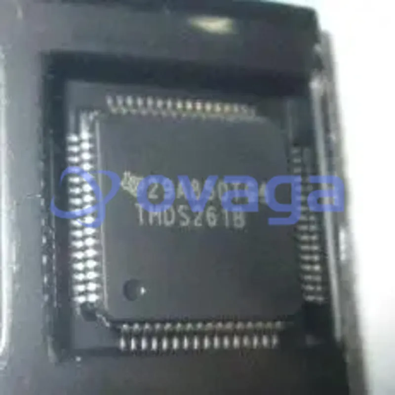
$5000TI TMDS261B
3-Gbps 2-to-1 HDMI/DVI mux with adaptive equalization


TMDS261B 일반적인 설명
The TMDS261B is a two-port digital video interface (DVI) or high-definition multimedia interface (HDMI) switch that allows up to two DVI or HDMI ports to be switched to a single display terminal. Four TMDS channels, one hot-plug detector, and a digital display control (DDC) interface are supported on each port. Each TMDS channel supports signaling rates up to 3 Gbps to allow 1080p resolution in 16-bit color depth. TMDS261B device is not intended for source side applications such as external switch boxes
The TMDS261B provides an adaptive equalizer for different ranges of cable lengths. The equalizer automatically compensates for intersymbol interference [ISI] loss of an HDMI/DVI cable for up to 20 dB at 3 Gbps (see ).
DLP is a trademark of Texas Instruments.
When any of the input ports are selected, the integrated terminations (50-Ω termination resistors pulled up to VCC) are switched on for the TMDS clock channel, the TMDS clock-detection circuit is enabled, and the DDC repeater is enabled. After a valid TMDS clock is detected, the integrated termination resistors for the data lines are enabled, and the output TMDS lines are enabled. When an input port is not selected, the integrated terminations are switched off, the TMDS receivers are disabled, and the DDC repeater is disabled. Clock-detection circuitry provides an automatic power-management feature, because if no valid TMDS clock is detected, the terminations on the input TMDS data lines are disconnected and the TMDS outputs are placed in a high-impedance state.
The TMDS261B is designed to be controlled via a local I2C interface or GPIO interface, based on the status of the I2C_SEL pin. The local I2C interface in TMDS261B is a slave-only I2C interface. (See the section.)
I2C Mode: When the I2C_SEL pin is set low, the device is in I2C mode. With local I2C, the interface port status can be read, and the advanced configurations of the device such as TMDS output edge rate control, DDC I2C buffer output-voltage-select (OVS) settings (See the for detailed description on DDC I2C buffer description and OVS description), device power management, TMDS clock-detect feature, and TMDS input-port selection can be set
GPIO mode: When the I2C_SEL pin is set high, the device is in GPIO control mode. The port selection is controlled with source selectors, S1 and S2. The power-saving mode is controlled through the LP pin. In GPIO mode, the default TMDS output edge rate that is the fastest setting of rise and fall time is set, and the default DDC I2C buffer OVS setting (OVS3) is set. See and the for a detailed description of the DDC I2C buffer.
Following are some of the key features (advantages) that the TMDS261B provides to the overall sink-side system (HDTV).
- 2×1 switch that supports TMDS data rates up to 3 Gbps on both input ports.
- ESD: Built-in support for high ESD protection (up to 10 kV on the HDMI source side). The HDMI source-side pins on the TMDS261B are connected via the HDMI/DVI exterior connectors and cable to the HDMI/DVI sources (e.g., DVD player). In TV applications, it can be expected that the source side may be subjected to higher ESD stresses compared to the sink side that is connected internally to the HDMI receiver.
- Adaptive equalization: The built-in adaptive equalization support compensates for intersymbol interference [ISI] loss of up to 20 dB, which represents a typical 20-m HDMI/DVI cable at 3 Gbps. Adaptive equalization adjusts the equalization gain automatically, based on the cable length and the incoming TMDS data rate.
- TMDS clock-detect circuitry: This feature provides an automatic power-management feature and also ensures that the TMDS output port is turned on only if there is a valid TMDS input signal. The TMDS clock-detect feature can be by-passed in I2C mode; see and . It is recommended to enable TMDS clock-detect circuitry during normal operation. However, for HDMI compliance testing (TMDS termination-voltage test), the clock-detect feature should be disabled by using the I2C mode control. If the customer requires passing the TMDS termination-voltage test in the GPIO mode with the default TMDS clock-detect circuitry enabled, then a valid TMDS clock should be provided for this compliance test, so that the terminations on the TMDS data pair can be connected and thus customer can pass the TMDS termination-voltage test.
- DDC I2C buffer: This feature provides isolation on the source-side and sink-side DDC I2C capacitance, thus helping the sink system to pass system-level compliance.
- Robust TMDS receive stage: This feature ensures that the TMDS261B can work with TMDS input signals having common-mode voltage levels that can be either compliant or non-compliant with HDMI/DVI specifications.
- VSadj: This feature adjusts the TMDS output swing and can help the sink system to tune the output TMDS swing of the TMDS261B (if needed) based on the system requirements.
- GPIO or local I2C interface to control the device features
- TMDS output edge-rate control: This feature adjusts the TMDS261B TMDS output rise and fall times. There are four settings of the rise and fall times that can be chosen. The default setting is the fastest rise and fall time; the other three settings are slower. Slower edge transitions can potentially help the sink system (HDTV) in passing regulatory EMI compliance.
특징
- 2:1 Sink-side switch Supporting DVI Above 1920 × 1200
and HDMI HDTV Resolutions up to 1080p With 16-Bit Color Depth - Designed for Signaling Rates up to 3 Gbps
- Supports HDMI 1.3a Specification
- Adaptive Equalization on inputs to support up to 20-m HDMI Cable
at 2.25 Gbps for 1080p 12-Bit Color Depth - TMDS Input Clock-Detect Circuit
- DDC Repeater Function
- <2-mW Low-Power Mode
- Local I2C or GPIO Configurable
- Enhanced ESD. HBM: 10 kV on All Input TMDS, DDC I2C, HPD Pins
- 3.3-Volt Power Supply
- Temperature Range: 0°C to 70°C
- 64-Pin TQFP Package: Pin-Compatible With TMDS251
- Robust TMDS Receive Stage That Can Work With Non-Compliant Input
Common-Mode HDMI Signal - APPLICATIONS
- High-Definition Digital TV
- LCD
- Plasma
- DLP
- High-Definition Digital TV
DLP is a trademark of Texas Instruments.
배송
| 배송 유형 | 배송비 | 리드타임 | |
|---|---|---|---|
 |
DHL | $20.00-$40.00 (0.50 KG) | 2-5 날 |
 |
페덱스 | $20.00-$40.00 (0.50 KG) | 2-5 날 |
 |
UPS | $20.00-$40.00 (0.50 KG) | 2-5 날 |
 |
TNT | $20.00-$40.00 (0.50 KG) | 2-5 날 |
 |
EMS | $20.00-$40.00 (0.50 KG) | 2-5 날 |
 |
등기 항공 우편 | $20.00-$40.00 (0.50 KG) | 2-5 날 |
처리 시간: 배송비는 지역 및 국가에 따라 다릅니다.
지불
| 지불 조건 | 핸드 수수료 | |
|---|---|---|
 |
은행 송금 | US$30.00의 은행 수수료를 부과합니다. |
 |
페이팔 | 4.0%의 서비스 수수료를 부과합니다. |
 |
신용 카드 | 3.5% 서비스 수수료를 부과합니다. |
 |
웨스턴 유니언 | charge US.00 banking fee. |
 |
돈 그램 | US$0.00의 은행 수수료를 부과합니다. |
보증
1. 귀하가 구입한 전자 부품에는 365일 보증이 포함되어 있으며, 우리는 제품 품질을 보장합니다.
2. 귀하가 받은 품목 중 일부가 완벽한 품질이 아닌 경우, 당사는 책임 있게 귀하의 환불 또는 교체를 준비할 것입니다. 그러나 품목은 원래 상태를 유지해야 합니다.
포장
-

단계1 :제품
-

단계2 :진공 포장
-

단계3 :정전기 방지 가방
-

단계4 :개별 포장
-

단계5 :포장 상자
-

단계6 :바코드 배송 태그


모든 제품은 정전기 방지 가방에 포장됩니다. ESD 정전기 방지 보호 장치와 함께 배송됩니다.
외부 ESD 포장 라벨은 당사 정보(부품 번호, 브랜드 및 수량)를 사용합니다.
우리는 선적 전에 모든 상품을 검사하고, 모든 제품이 양호한 상태인지 확인하고, 부품이 새로운 원본 일치 데이터시트인지 확인합니다.
모든 상품을 포장한 후 문제가 없는지 확인한 후 안전하게 포장하여 글로벌 특급으로 보내드립니다. 우수한 밀봉 무결성과 함께 탁월한 천공 및 인열 저항성을 나타냅니다.


우리는 고품질 제품, 사려 깊은 서비스 및 판매 후 보증을 제공합니다.
-

우리는 풍부한 제품을 보유하고 있으며 귀하의 다양한 요구를 충족시킬 수 있습니다.
-

최소 주문 수량은 1개부터입니다.
-

최저 국제 배송비는 $0.00부터 시작됩니다
-

모든 제품에 대해 365일 품질 보증


