

이미지는 참고용입니다. 제품 사양 보기
ON NC7WV07P6X
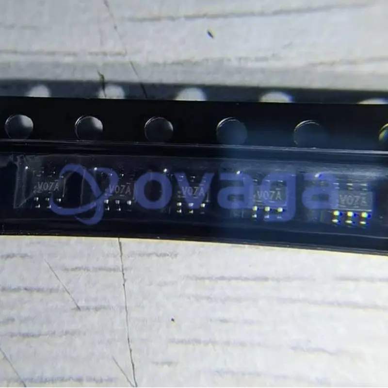
Buffer, Non-Inverting 2 Element 1 Bit per Element Open Drain Output SC-88 (SC-70-6)


NC7WV07P6X 일반적인 설명
The NC7WV07 is a dual buffer with open drain output from ON Semiconductor's Ultra Low Power-A series of TinyLogic®. ULP-A is ideal for applications that require extreme high speed, high drive and low power. This product is designed for a wide low voltage operating range (0.9V to 3.6V VCC) and applications that require more drive and speed than the TinyLogic ULP series, but still offer best in class low power operation.
The NC7WV07 is uniquely designed for optimized power and speed, and is fabricated with an advanced CMOS technology to achieve high-speed operation while maintaining low CMOS power dissipation.
특징
- 0.9V to 3.6V VCC supply operation
- 3.6V overvoltage tolerant I/O's at VCC from 0.9V to 3.6V
- Extremely High Speed tPD1.0 ns typ for 2.7V to 3.6V VCC1.2 ns typ for 2.3V to 2.7V VCC2.0 ns typ for 1.65V to 1.95V VCC3.2 ns typ for 1.4V to 1.6V VCC6.0 ns typ for 1.1V to 1.3V VCC13.0 ns typ for 0.9V VCC
- Power-Off high impedance inputs and outputs
- High Static Drive (IOH/IOL)±24 mA @ 3.00V VCC±18 mA @ 2.30V VCC±6 mA @ 1.65V VCC±4 mA @ 1.4V VCC±2 mA @ 1.1V VCC±0.1 mA @ 0.9V VCC
- Uses patented Quiet Series™ noise/EMI reduction circuitry
- Ultra small MicroPak™ leadfree package
- Ultra low dynamic power
애플리케이션
- This product is general usage and suitable for many different applications.
명세서
| 매개변수 | 값 | 매개변수 | 값 |
|---|---|---|---|
| Source Content uid | NC7WV07P6X | Pbfree Code | Yes |
| Part Life Cycle Code | Active | Ihs Manufacturer | ONSEMI |
| Package Description | SC-88, 6 PIN | Manufacturer Package Code | 419AD |
| Reach Compliance Code | compliant | HTS Code | 8542.39.00.01 |
| Factory Lead Time | 75 Weeks, 5 Days | Samacsys Manufacturer | onsemi |
| Family | AUP/ULP/V | JESD-30 Code | R-PDSO-G6 |
| Logic IC Type | BUFFER | Moisture Sensitivity Level | 1 |
| Number of Functions | 2 | Number of Inputs | 1 |
| Number of Terminals | 6 | Output Characteristics | OPEN-DRAIN |
| Package Body Material | PLASTIC/EPOXY | Package Code | TSSOP |
| Package Equivalence Code | TSSOP6,.08 | Package Shape | RECTANGULAR |
| Package Style | SMALL OUTLINE, THIN PROFILE, SHRINK PITCH | Packing Method | TR |
| Peak Reflow Temperature (Cel) | 260 | Schmitt Trigger | NO |
| Surface Mount | YES | Technology | CMOS |
| Terminal Finish | NICKEL PALLADIUM GOLD | Terminal Form | GULL WING |
| Terminal Position | DUAL | Time@Peak Reflow Temperature-Max (s) | 30 |
| feature-logic-family | WV | feature-logic-function | Buffer/Driver |
| feature-number-of-elements-per-chip | 2 | feature-process-technology | CMOS |
| feature-maximum-low-level-output-current-ma | 24 | feature-output-type | Open Drain |
| feature-minimum-operating-supply-voltage-v | 0.9 | feature-maximum-operating-supply-voltage-v | 3.6 |
| feature-maximum-high-level-output-current-ma | -24 | feature-packaging | Tape and Reel |
| feature-rad-hard | feature-pin-count | 6 | |
| feature-supplier-package | SC-70 | feature-standard-package-name1 | SOT |
| feature-cecc-qualified | No | feature-esd-protection | |
| feature-military | No | feature-aec-qualified | No |
| feature-aec-qualified-number | feature-auto-motive | No | |
| feature-p-pap | No | feature-eccn-code | EAR99 |
| feature-svhc | No |
배송
| 배송 유형 | 배송비 | 리드타임 | |
|---|---|---|---|
 |
DHL | $20.00-$40.00 (0.50 KG) | 2-5 날 |
 |
페덱스 | $20.00-$40.00 (0.50 KG) | 2-5 날 |
 |
UPS | $20.00-$40.00 (0.50 KG) | 2-5 날 |
 |
TNT | $20.00-$40.00 (0.50 KG) | 2-5 날 |
 |
EMS | $20.00-$40.00 (0.50 KG) | 2-5 날 |
 |
등기 항공 우편 | $20.00-$40.00 (0.50 KG) | 2-5 날 |
처리 시간: 배송비는 지역 및 국가에 따라 다릅니다.
지불
| 지불 조건 | 핸드 수수료 | |
|---|---|---|
 |
은행 송금 | US$30.00의 은행 수수료를 부과합니다. |
 |
페이팔 | 4.0%의 서비스 수수료를 부과합니다. |
 |
신용 카드 | 3.5% 서비스 수수료를 부과합니다. |
 |
웨스턴 유니언 | charge US.00 banking fee. |
 |
돈 그램 | US$0.00의 은행 수수료를 부과합니다. |
보증
1. 귀하가 구입한 전자 부품에는 365일 보증이 포함되어 있으며, 우리는 제품 품질을 보장합니다.
2. 귀하가 받은 품목 중 일부가 완벽한 품질이 아닌 경우, 당사는 책임 있게 귀하의 환불 또는 교체를 준비할 것입니다. 그러나 품목은 원래 상태를 유지해야 합니다.
포장
-

단계1 :제품
-

단계2 :진공 포장
-

단계3 :정전기 방지 가방
-

단계4 :개별 포장
-

단계5 :포장 상자
-

단계6 :바코드 배송 태그


모든 제품은 정전기 방지 가방에 포장됩니다. ESD 정전기 방지 보호 장치와 함께 배송됩니다.
외부 ESD 포장 라벨은 당사 정보(부품 번호, 브랜드 및 수량)를 사용합니다.
우리는 선적 전에 모든 상품을 검사하고, 모든 제품이 양호한 상태인지 확인하고, 부품이 새로운 원본 일치 데이터시트인지 확인합니다.
모든 상품을 포장한 후 문제가 없는지 확인한 후 안전하게 포장하여 글로벌 특급으로 보내드립니다. 우수한 밀봉 무결성과 함께 탁월한 천공 및 인열 저항성을 나타냅니다.


부품 포인트
-
The NC7WV07P6X chip is a triple buffer gate that can be used for level shifting signals in various electronic circuits. It has three inputs and three outputs and operates at a supply voltage of 1.65V to 5.5V. The chip is designed to provide high-speed signal buffering while consuming very low power, making it suitable for applications in portable devices and battery-powered systems.
-
Equivalent
There aren't any exact equivalent products to the NC7WV07P6X chip. However, some similar alternatives you may consider are the SN74LV07A, TC7WG07FK, and HCT07 chips, as they have similar functionalities and specifications. -
Features
The NC7WV07P6X is a dual buffer/line driver that operates from rail-to-rail voltage signals with a wide operating voltage range. It offers low power consumption, high-speed operation, and is designed with Schmitt-trigger inputs to provide noise immunity. It also has balanced input and output characteristics and supports overvoltage-tolerant input levels, making it suitable for various applications. -
Pinout
The NC7WV07P6X is a single logic gate with an open-drain output. It has a pin count of 6, which includes one input pin, one output pin, and four power supply/GND pins. The open-drain output allows for bi-directional signal transmission and is commonly used for level shifting applications. -
Manufacturer
The manufacturer of the NC7WV07P6X is ON Semiconductor. ON Semiconductor is a multinational company specializing in the design and production of semiconductors and integrated circuits for various industries, including automotive, communications, computing, and consumer electronics. -
Application Field
The NC7WV07P6X is a voltage-level translator used for translating voltage levels between different logic families. It can be applied in various applications such as battery-powered portable devices, mobile phones, digital cameras, and other electronics requiring voltage translation between different logic levels. -
Package
The NC7WV07P6X chip has a package type of SC-70, a form of SMD (Surface Mount Device), and a size of 2.00mm x 2.10mm x 1.20mm.


데이터 시트 PDF
우리는 고품질 제품, 사려 깊은 서비스 및 판매 후 보증을 제공합니다.
-

우리는 풍부한 제품을 보유하고 있으며 귀하의 다양한 요구를 충족시킬 수 있습니다.
-

최소 주문 수량은 1개부터입니다.
-

최저 국제 배송비는 $0.00부터 시작됩니다
-

모든 제품에 대해 365일 품질 보증


We will definitely be purchasing from Ovaga in the future.