이미지는 참고용입니다. 제품 사양 보기
주문 금액이
$5000LFXP2-8E-5TN144I
FPGA with 8K LUTs and 100 I/O instances for DSP applications at 1.2V and -5 speed grade


LFXP2-8E-5TN144I 일반적인 설명
Lattice Semiconductor's LFXP2-8E-5TN144I is a standout member of the LatticeXP2 family, offering impressive features in a compact form factor. With its high logic capacity, low-power design, and support for various I/O standards, this FPGA provides a versatile and efficient solution for a wide range of applications. Its high-speed performance and embedded memory blocks make it a compelling choice for projects that require quick data processing and storage
특징
- The LFXP2-8E-5TN144I has a unique architecture that supports parallel processing
- This enables high-speed data transfer between different parts of the FPGA
- The device also includes advanced power management features
- This enables efficient use of energy and reduces heat generation
- The LFXP2-8E-5TN144I is suitable for a wide range of applications
애플리케이션
- Small but mighty
- Powerful and efficient
- Perfect for IoT
명세서
| 매개변수 | 값 | 매개변수 | 값 |
|---|---|---|---|
| Product Category | FPGA - Field Programmable Gate Array | RoHS | Details |
| Series | LFXP2 | Number of Logic Elements | 8000 LE |
| Adaptive Logic Modules - ALMs | 4000 ALM | Embedded Memory | 221 kbit |
| Number of I/Os | 100 I/O | Supply Voltage - Min | 1.14 V |
| Supply Voltage - Max | 1.26 V | Minimum Operating Temperature | - 40 C |
| Maximum Operating Temperature | + 100 C | Mounting Style | SMD/SMT |
| Package / Case | TQFP-144 | Brand | Lattice |
| Distributed RAM | 18 kbit | Embedded Block RAM - EBR | 221 kbit |
| Height | 1.4 mm | Length | 20 mm |
| Maximum Operating Frequency | 311 MHz | Moisture Sensitive | Yes |
| Number of Logic Array Blocks - LABs | 1000 LAB | Operating Supply Voltage | 1.2 V |
| Product Type | FPGA - Field Programmable Gate Array | Factory Pack Quantity | 60 |
| Subcategory | Programmable Logic ICs | Total Memory | 239 kbit |
| Width | 20 mm |
배송
| 배송 유형 | 배송비 | 리드타임 | |
|---|---|---|---|
 |
DHL | $20.00-$40.00 (0.50 KG) | 2-5 날 |
 |
페덱스 | $20.00-$40.00 (0.50 KG) | 2-5 날 |
 |
UPS | $20.00-$40.00 (0.50 KG) | 2-5 날 |
 |
TNT | $20.00-$40.00 (0.50 KG) | 2-5 날 |
 |
EMS | $20.00-$40.00 (0.50 KG) | 2-5 날 |
 |
등기 항공 우편 | $20.00-$40.00 (0.50 KG) | 2-5 날 |
처리 시간: 배송비는 지역 및 국가에 따라 다릅니다.
지불
| 지불 조건 | 핸드 수수료 | |
|---|---|---|
 |
은행 송금 | US$30.00의 은행 수수료를 부과합니다. |
 |
페이팔 | 4.0%의 서비스 수수료를 부과합니다. |
 |
신용 카드 | 3.5% 서비스 수수료를 부과합니다. |
 |
웨스턴 유니언 | charge US.00 banking fee. |
 |
돈 그램 | US$0.00의 은행 수수료를 부과합니다. |
보증
1. 귀하가 구입한 전자 부품에는 365일 보증이 포함되어 있으며, 우리는 제품 품질을 보장합니다.
2. 귀하가 받은 품목 중 일부가 완벽한 품질이 아닌 경우, 당사는 책임 있게 귀하의 환불 또는 교체를 준비할 것입니다. 그러나 품목은 원래 상태를 유지해야 합니다.
포장
-

단계1 :제품
-

단계2 :진공 포장
-

단계3 :정전기 방지 가방
-

단계4 :개별 포장
-

단계5 :포장 상자
-

단계6 :바코드 배송 태그


모든 제품은 정전기 방지 가방에 포장됩니다. ESD 정전기 방지 보호 장치와 함께 배송됩니다.
외부 ESD 포장 라벨은 당사 정보(부품 번호, 브랜드 및 수량)를 사용합니다.
우리는 선적 전에 모든 상품을 검사하고, 모든 제품이 양호한 상태인지 확인하고, 부품이 새로운 원본 일치 데이터시트인지 확인합니다.
모든 상품을 포장한 후 문제가 없는지 확인한 후 안전하게 포장하여 글로벌 특급으로 보내드립니다. 우수한 밀봉 무결성과 함께 탁월한 천공 및 인열 저항성을 나타냅니다.


부품 포인트
-
The LFXP2-8E-5TN144I chip is a low-cost and low-power FPGA (Field-Programmable Gate Array) from Lattice Semiconductor aimed at applications requiring high-performance and flexibility. With 2,320 LUTs and 10,000 logic elements, this chip offers a versatile platform for implementing various designs and algorithms. Its compact size and low power consumption make it suitable for embedded systems and IoT applications.
-
Equivalent
The equivalent products of LFXP2-8E-5TN144I chip are LFE2-8E-5TN144, LFE2-8E-6TN, and LFE2-8E-7FT256. These chips are from the same Lattice Semiconductor family and have similar features and functionality, making them suitable replacements for the LFXP2-8E-5TN144I chip. -
Features
The LFXP2-8E-5TN144I is a low-power, small-footprint FPGA with 1550 logic elements, 48 Kbits of block RAM, and 37 user I/Os. It features Flash*Freeze technology for ultra-low static power consumption, In-System Programming (ISP) capability, and reconfigurable logic module (RLM) blocks for flexible design implementation. -
Pinout
The LFXP2-8E-5TN144I is a 144-pin FPGA (field-programmable gate array) with 8K LUTs and 108 I/Os. It is used for implementing digital logic circuits and customizing functions. The pin count refers to the number of I/O pins connecting the device to external components for input and output operations. -
Manufacturer
The manufacturer of the LFXP2-8E-5TN144I is Lattice Semiconductor Corporation. It is a technology company that specializes in semiconductor design and manufacturing. Lattice Semiconductor Corporation focuses on developing programmable logic devices, software, and related intellectual property to help customers build innovative products across a wide range of markets. -
Application Field
The LFXP2-8E-5TN144I is suitable for various applications such as industrial automation, medical devices, consumer electronics, communication systems, and automotive electronics. It is an ideal choice for applications that require low power consumption, high performance, and flexibility in a compact form factor. -
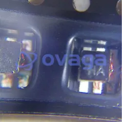
Package
The LFXP2-8E-5TN144I chip is in a 144-pin TQFP (Thin Quad Flat Package) form, which measures 14mm x 14mm. The package size is 16mm x 16mm x 1.4mm, and it has 144 pins in a 12x12 grid array.


우리는 고품질 제품, 사려 깊은 서비스 및 판매 후 보증을 제공합니다.
-

우리는 풍부한 제품을 보유하고 있으며 귀하의 다양한 요구를 충족시킬 수 있습니다.
-

최소 주문 수량은 1개부터입니다.
-

최저 국제 배송비는 $0.00부터 시작됩니다
-

모든 제품에 대해 365일 품질 보증