이미지는 참고용입니다. 제품 사양 보기
주문 금액이
$5000LCMXO3LF-1300C-5BG256I
This FPGA operates at a voltage of 1.2V and comes in a 256-pin chip-scale package (CABGA) configuration, delivered in a tray format


브랜드: Lattice Semiconductor Corporation
제조업체부품 #: LCMXO3LF-1300C-5BG256I
데이터 시트: LCMXO3LF-1300C-5BG256I 데이터 시트 (PDF)
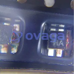
패키지/케이스: 256-LFBGA
LCMXO3LF-1300C-5BG256I 일반적인 설명
The LCMXO3LF-1300C-5BG256I FPGA, manufactured by Lattice Semiconductor, offers a compelling combination of performance and energy efficiency. With a logic cell count of 1300 and a maximum speed grade of 5, this low-cost, low-power FPGA is capable of handling small to medium-sized designs with ease. Its 256-pin BGA package ensures a compact form factor, making it a great fit for space-constrained applications, while its low power consumption makes it ideal for mobile devices, IoT applications, and other battery-powered devices. Additionally, the LCMXO3LF-1300C-5BG256I boasts embedded block RAM, DSP blocks, and flexible I/O options, allowing for versatile and efficient design implementations across a wide range of applications
특징
- Non-volatile, Infinitely Reconfigurable
- Instant-on – powers up in microseconds
- Single chip, no external configuration memory
- required
- Excellent design security, no bit stream to
- intercept
- Reconfigure SRAM based logic in milliseconds
- SRAM and non-volatile memory programmable
- through JTAG port
- Supports background programming of
- non-volatile memory
- Sleep Mode
- Allows up to 100x static current reduction
- TransFR™ Reconfiguration (TFR)
- In-field logic update while system operates
- High I/O to Logic Density
- 256 to 2280 LUT4s
- 73 to 271 I/Os with extensive package options
- Density migration supported
- Lead free/RoHS compliant packaging
- Embedded and Distributed Memory
- Up to 27.6 Kbits sysMEM™ Embedded Block
- Up to 7.5 Kbits distributed RAM
- Dedicated FIFO control logic
- Flexible I/O Buffer
- Programmable sysIO™ buffer supports wide
- range of interfaces:
- − LVCMOS 3.3/2.5/1.8/1.5/1.2
- − LVTTL
- − LVDS, Bus-LVDS, LVPECL, RSDS
- sysCLOCK™ PLLs
- Up to two analog PLLs per device
- Clock multiply, divide, and phase shifting
- System Level Support
- IEEE Standard 1149.1 Boundary Scan
- Onboard oscillator
- Devices operate with 3.3V, 2.5V, 1.8V or 1.2V
- power supply
- IEEE 1532 compliant in-system programming
명세서
| 매개변수 | 값 | 매개변수 | 값 |
|---|---|---|---|
| Series | MachXO3 | Package | Tray |
| Product Status | Active | Programmabe | Not Verified |
| Number of LABs/CLBs | 160 | Number of Logic Elements/Cells | 1280 |
| Total RAM Bits | 65536 | Number of I/O | 206 |
| Voltage - Supply | 2.375V ~ 3.465V | Mounting Type | Surface Mount |
| Operating Temperature | -40°C ~ 100°C (TJ) | Package / Case | 256-LFBGA |
| Supplier Device Package | 256-CABGA (14x14) |
배송
| 배송 유형 | 배송비 | 리드타임 | |
|---|---|---|---|
 |
DHL | $20.00-$40.00 (0.50 KG) | 2-5 날 |
 |
페덱스 | $20.00-$40.00 (0.50 KG) | 2-5 날 |
 |
UPS | $20.00-$40.00 (0.50 KG) | 2-5 날 |
 |
TNT | $20.00-$40.00 (0.50 KG) | 2-5 날 |
 |
EMS | $20.00-$40.00 (0.50 KG) | 2-5 날 |
 |
등기 항공 우편 | $20.00-$40.00 (0.50 KG) | 2-5 날 |
처리 시간: 배송비는 지역 및 국가에 따라 다릅니다.
지불
| 지불 조건 | 핸드 수수료 | |
|---|---|---|
 |
은행 송금 | US$30.00의 은행 수수료를 부과합니다. |
 |
페이팔 | 4.0%의 서비스 수수료를 부과합니다. |
 |
신용 카드 | 3.5% 서비스 수수료를 부과합니다. |
 |
웨스턴 유니언 | charge US.00 banking fee. |
 |
돈 그램 | US$0.00의 은행 수수료를 부과합니다. |
보증
1. 귀하가 구입한 전자 부품에는 365일 보증이 포함되어 있으며, 우리는 제품 품질을 보장합니다.
2. 귀하가 받은 품목 중 일부가 완벽한 품질이 아닌 경우, 당사는 책임 있게 귀하의 환불 또는 교체를 준비할 것입니다. 그러나 품목은 원래 상태를 유지해야 합니다.
포장
-

단계1 :제품
-

단계2 :진공 포장
-

단계3 :정전기 방지 가방
-

단계4 :개별 포장
-

단계5 :포장 상자
-

단계6 :바코드 배송 태그


모든 제품은 정전기 방지 가방에 포장됩니다. ESD 정전기 방지 보호 장치와 함께 배송됩니다.
외부 ESD 포장 라벨은 당사 정보(부품 번호, 브랜드 및 수량)를 사용합니다.
우리는 선적 전에 모든 상품을 검사하고, 모든 제품이 양호한 상태인지 확인하고, 부품이 새로운 원본 일치 데이터시트인지 확인합니다.
모든 상품을 포장한 후 문제가 없는지 확인한 후 안전하게 포장하여 글로벌 특급으로 보내드립니다. 우수한 밀봉 무결성과 함께 탁월한 천공 및 인열 저항성을 나타냅니다.


부품 포인트
-
The LCMXO3LF-1300C-5BG256I chip is a low-power, small-footprint FPGA (field-programmable gate array) from Lattice Semiconductor. It features 1300 LUTs, 317 Kbits of embedded memory, and 36 I/Os. This chip is ideal for applications requiring low power consumption and space constraints.
-
Equivalent
The equivalent products of the LCMXO3LF-1300C-5BG256I chip are the LCMXO3 series from Lattice Semiconductor, including the LCMXO3LF-1300C-6BG256I and the LCMXO3LF-1300C-6BG324I. These chips offer similar features and functionality, providing alternative options for design and integration. -
Features
LCMXO3LF-1300C-5BG256I features 1300 LUTs, 640 macrocells, 6 kilobits of RAM, 32 I/Os, and is housed in a 256-ball grid array package. It has low power consumption, small form factor, and is ideal for low power applications in industrial, consumer, and automotive markets. -
Pinout
The LCMXO3LF-1300C-5BG256I is a low-power FPGA with 256 pins. It is designed for use in low-power applications and features 1300 LUTs. It also includes 4 Multiplier/Accumulators and 32 I/O pins. -
Manufacturer
LCMXO3LF-1300C-5BG256I is manufactured by Lattice Semiconductor Corporation, a company specializing in low-power, small form-factor programmable logic devices. Lattice Semiconductor Corporation is a leading provider of smart connectivity solutions, offering customizable solutions for a wide range of applications in consumer, automotive, industrial, and communications markets. -
Application Field
The LCMXO3LF-1300C-5BG256I can be used in a variety of application areas such as battery management systems, sensor interfaces, portable medical devices, and industrial automation. Its low power consumption, small form factor, and high integration make it ideal for applications requiring low power consumption and high performance in a compact package. -
Package
The LCMXO3LF-1300C-5BG256I chip is in a 256-ball Fine-pitch Ball Grid Array (FPBGA) package. It is a Field-Programmable Gate Array (FPGA) in a form of a chip. The size of the chip is 13mm x 13mm.


우리는 고품질 제품, 사려 깊은 서비스 및 판매 후 보증을 제공합니다.
-

우리는 풍부한 제품을 보유하고 있으며 귀하의 다양한 요구를 충족시킬 수 있습니다.
-

최소 주문 수량은 1개부터입니다.
-

최저 국제 배송비는 $0.00부터 시작됩니다
-

모든 제품에 대해 365일 품질 보증