


이미지는 참고용입니다. 제품 사양 보기
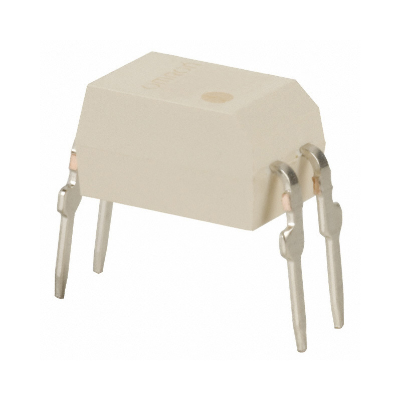
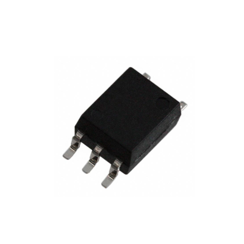
CD4016BE
100-pA on-state leakage current, 20-V, 1:1 (SPST), 4-channel analog switch


CD4016BE 일반적인 설명
CD4016B Series types are quad bilateral switches intended for the transmission or multiplexing of analog or digital signals. Each of the four independent bilateral switches has a single control signal input which simultaneously biases both the p and n device in a given switch on or off.
The CD4016 "B" Series types are supplied in 14-lead hermetic dual-in-line ceramic packages (F3A suffix), 14-lead dual-in-line plastic packages (E suffix), 14-lead small-outline packages (M, MT, M96, and NSR suffixes), and 14-lead thin shrink small-outline packages (PW and PWR suffixes).
특징
- 20-V digital or ± 10-V peak-to-peak switching
- 280- typical on-state resistance for 15-V operation
- Switch on-state resistance matched to within 10 typ. over 15-V signal-input range
- High on/off output-voltage ratio:
65 dB typ. @ fis = 10 kHz, RL = 10 k - High degree of linearity:
<0.5% distortion typ. @ fis = 1 kHz, Vis = 5 Vp-p, VDD–VSS - Extremely low off-state switch leakage resulting in very low offset current and high effective off-state resistance:
100pA typ. @ VDD–VSS = 18 V, TA = 25°C - Extremely high control input impedance (control circuit isolated form signal circuit:
1012typ. - Low crosstalk between switches:
–50 dB typ. @ fis= 0.9 MHz, RL = 1 k - Matched control-input to signal-output capacitance:
Reduces output signal transients - Frequency response, switch on = 40MHz (typ.)
- 100% tested for quiescent current at 20 V
- Maximum control input current of 1 µA at 18 V over full package temperature range; 100 nA at 18 V and 25°C
- 5-V, 10-V, and 15-V parametric ratings
- Applications:
- Analog signal switching/multiplexing
- Signal gating
- Squelch control
- Chopper
- Modulator
- Demodulator
- Commutating switch
- Digital signal switching/multiplexing
- CMOS logic implementation
- Analog-to-digital & digital-to-analog conversion
- Digital control of frequency, impedance, phase, and analog-signal gain
- Analog signal switching/multiplexing
Data sheet acquired from Harris Semiconductor
명세서
| 매개변수 | 값 | 매개변수 | 값 |
|---|---|---|---|
| Configuration | 1:1 SPST | Number of channels | 4 |
| Power supply voltage - single (V) | 3.3, 5, 12, 16, 20 | Power supply voltage - dual (V) | +/-10, +/-2.5, +/-5 |
| Protocols | Analog | Ron (typ) (Ω) | 180 |
| CON (typ) (pF) | 4 | Supply current (typ) (µA) | 0.01 |
| Bandwidth (MHz) | 40 | Operating temperature range (°C) | -55 to 125 |
| Features | Break-before-make | Input/output continuous current (max) (mA) | 10 |
| Rating | Catalog | Drain supply voltage (max) (V) | 18 |
| Supply voltage (max) (V) | 18 |
배송
| 배송 유형 | 배송비 | 리드타임 | |
|---|---|---|---|
 |
DHL | $20.00-$40.00 (0.50 KG) | 2-5 날 |
 |
페덱스 | $20.00-$40.00 (0.50 KG) | 2-5 날 |
 |
UPS | $20.00-$40.00 (0.50 KG) | 2-5 날 |
 |
TNT | $20.00-$40.00 (0.50 KG) | 2-5 날 |
 |
EMS | $20.00-$40.00 (0.50 KG) | 2-5 날 |
 |
등기 항공 우편 | $20.00-$40.00 (0.50 KG) | 2-5 날 |
처리 시간: 배송비는 지역 및 국가에 따라 다릅니다.
지불
| 지불 조건 | 핸드 수수료 | |
|---|---|---|
 |
은행 송금 | US$30.00의 은행 수수료를 부과합니다. |
 |
페이팔 | 4.0%의 서비스 수수료를 부과합니다. |
 |
신용 카드 | 3.5% 서비스 수수료를 부과합니다. |
 |
웨스턴 유니언 | charge US.00 banking fee. |
 |
돈 그램 | US$0.00의 은행 수수료를 부과합니다. |
보증
1. 귀하가 구입한 전자 부품에는 365일 보증이 포함되어 있으며, 우리는 제품 품질을 보장합니다.
2. 귀하가 받은 품목 중 일부가 완벽한 품질이 아닌 경우, 당사는 책임 있게 귀하의 환불 또는 교체를 준비할 것입니다. 그러나 품목은 원래 상태를 유지해야 합니다.
포장
-

단계1 :제품
-

단계2 :진공 포장
-

단계3 :정전기 방지 가방
-

단계4 :개별 포장
-

단계5 :포장 상자
-

단계6 :바코드 배송 태그


모든 제품은 정전기 방지 가방에 포장됩니다. ESD 정전기 방지 보호 장치와 함께 배송됩니다.
외부 ESD 포장 라벨은 당사 정보(부품 번호, 브랜드 및 수량)를 사용합니다.
우리는 선적 전에 모든 상품을 검사하고, 모든 제품이 양호한 상태인지 확인하고, 부품이 새로운 원본 일치 데이터시트인지 확인합니다.
모든 상품을 포장한 후 문제가 없는지 확인한 후 안전하게 포장하여 글로벌 특급으로 보내드립니다. 우수한 밀봉 무결성과 함께 탁월한 천공 및 인열 저항성을 나타냅니다.


우리는 고품질 제품, 사려 깊은 서비스 및 판매 후 보증을 제공합니다.
-

우리는 풍부한 제품을 보유하고 있으며 귀하의 다양한 요구를 충족시킬 수 있습니다.
-

최소 주문 수량은 1개부터입니다.
-

최저 국제 배송비는 $0.00부터 시작됩니다
-

모든 제품에 대해 365일 품질 보증


